Semiconductor product and method for forming a semiconductor product

a semiconductor and product technology, applied in the field of semiconductor products and semiconductor products, can solve the problems of increasing the risk of misalignment and other critical parameters of semiconductor manufacturers, the inability to shrink microelectronic elements in semiconductor devices, and the need for new techniques for increasing the storage capacity of memory devices, etc., to achieve the effect of increasing the number of memory cells, increasing the storage capacity, and increasing the number of bits

Inactive Publication Date: 2007-05-17
INFINEON TECH AG
View PDF2 Cites 137 Cited by
  • Summary
  • Abstract
  • Description
  • Claims
  • Application Information

AI Technical Summary

Benefits of technology

[0007] In one aspect, the invention provides a semiconductor product having an increased storage capacity, that is, which comprises an increased number of memory cells and which is capable of storing an increased number of bits compared to prior art semiconductor products of equal lateral dimensions. In a further aspect, the present invention provides a semiconductor product enabling operating a memory array having an increased number of memory cells without any increase of the load capacitance and parasitic el

Problems solved by technology

However, the potential of shrinking microelectronic elements in semiconductor devices is limited to a certain extent, depending on a respective technology (typically addressed by the respective size of the gate length) and the size of a semiconductor wafer.
With increasing wafer diameter the risk of misalignments and other critical parameters in

Method used


Image

  • Semiconductor product and method for forming a semiconductor product
  • Semiconductor product and method for forming a semiconductor product
  • Semiconductor product and method for forming a semiconductor product

Examples


first embodiment

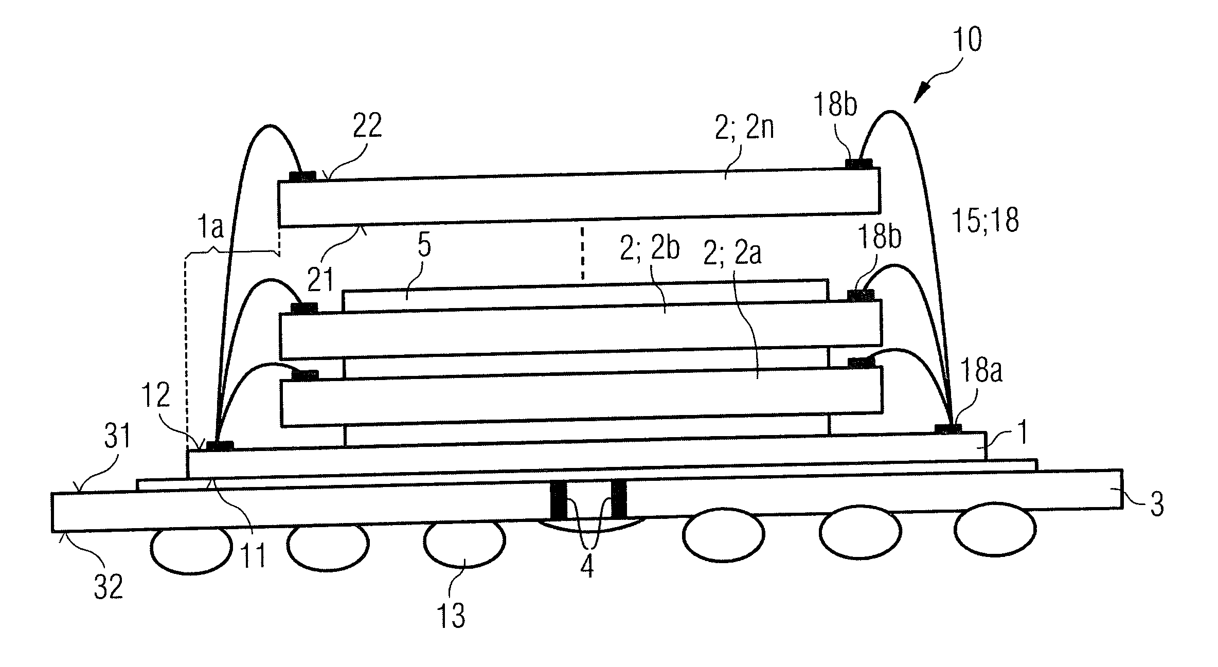
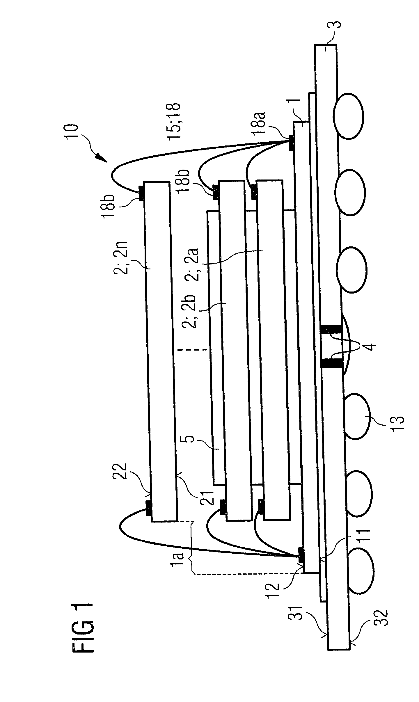
[0085]FIG. 1 illustrates a cross-sectional view of a semiconductor product of the invention. The semiconductor product 10 comprises one first semiconductor chip 1 and a plurality of equally sized second semiconductor chips 2; 2a, 2b, . . . , 2n stacked on one another and being supported by the first semiconductor chip 1. For stacking the first and second semiconductor chips 1, 2 to one another, adhesive layers 5 may be provided therebetween. The second semiconductor chips 2 each comprise at least one memory bank (not illustrated in FIG. 1) which memory banks for each second memory chip may extend over almost the entire upper main surface 22 of the respective second semiconductor chip (see FIG. 2). The first and second semiconductor chips 1, 2 may be made of silicon or any other semiconductor material, for instance, and each comprise an integrated circuit. The integrated circuit of the first semiconductor chip 1 essentially is formed of a input / output circuitry which, in a convention...

second embodiment

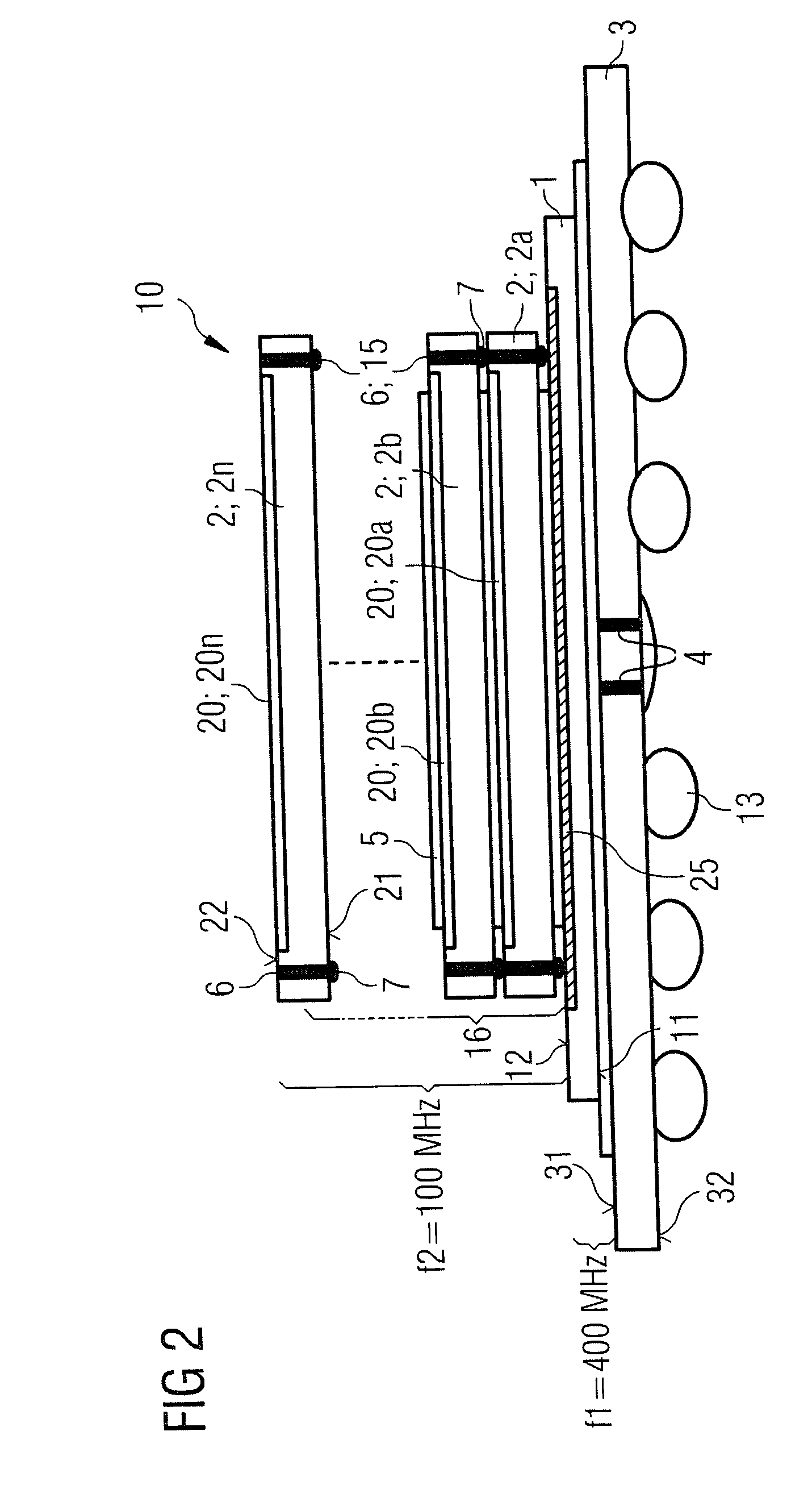
[0088]FIG. 2 illustrates a cross-sectional view of a semiconductor product of the present invention. According to FIG. 2, the second semiconductor chips 2 are stacked on one another and on the first semiconductor chip 1 by means of electrically conductive connecting means 15, which comprise through-hole fillings 6 and bond balls 7. Thereby no bond wires are required that would need to be provided laterally beyond the size of the second semiconductor chips 2. Each second semiconductor chip 2 comprises a plurality of through-holes that are filled with through-hole fillings 6 extending between the two respective main surfaces 21, 22 of the respective second semiconductor chip 2. The bond balls 7 are provided in spaces between two respective second semiconductor chips 2 so as to connect two through-hole fillings 6 to one another. Further elements illustrated in FIG. 2 correspond to those elements having the same reference numbers as indicated in FIG. 1.

[0089] In addition thereto, FIG. 2...

third embodiment

[0092]FIG. 3 illustrates a cross-sectional view of the invention. According to FIG. 3, the electrically conductive connecting means are comprising through-hole fillings 6 and bond balls 7 as in FIG. 2, again conductive columns 16 formed of through-hole fillings 6 and bond balls 7 arranged on top of one another in alternating order are provided. In contrast to FIG. 2, the electrically conductive connecting means 15 in FIG. 3 are provided in laterally centered positions of the second semiconductor chips 2 rather than at the edges of the second semiconductor chips 2. In particular, the bond balls 7 are provided in recesses of the adhesive layers 5. Accordingly, the conductive columns 16 may be arranged at any desired lateral position within the lateral extensions of the second semiconductor chips 2. Further elements illustrated in FIG. 3 correspond to those elements illustrated in FIGS. 1 and 2 having the same reference numbers. The exemplary operating frequencies illustrated in FIG. 2...


PUM


Abstract

A semiconductor product includes a first semiconductor chip that includes input/output circuitry enabling transfer of data from memory banks of the semiconductor product to an external electronic device and/or from an external electronic device to the memory banks of the semiconductor product. A number of second semiconductor chips are stacked on and electrically coupled to the first semiconductor chip. The second semiconductor chips are stacked on one another. Each second semiconductor chip of the plurality of second semiconductor chips comprises at least one of the memory banks of the semiconductor product. The memory banks of the second semiconductor chips are accessible by the input/output circuitry arranged on the first semiconductor chip.

Description

TECHNICAL FIELD [0001] The present invention relates generally to a semiconductor product and method for forming a semiconductor product. BACKGROUND [0002] The invention refers to a semiconductor product and to methods for forming a semiconductor product. Semiconductor products like memory products, in particular volatile memory products, comprise a memory array having a plurality of memory cells. In DRAMs (dynamical random access memories), for instance, memory cells accessible by read operations and write operations are provided in the memory array. The memory cells are arranged in rows and columns and are connected to wordlines and bitlines. [0003] Modern memory products comprise rather complex array architectures in which the memory array comprises a plurality of memory banks, the memory banks each comprising a respective plurality of memory cells and all memory banks being accessible in parallel to one another. For accessing the memory banks of the memory array, input / output ci...

Claims


Application Information

Patent Timeline
IPC IPC(8): G11C5/06
CPCH01L25/0657H01L2224/16225H01L2224/48091H01L2224/48227H01L2224/73265H01L2225/0651H01L2225/06513H01L2225/06517H01L2225/06541H01L2225/06575H01L2924/15311H01L2924/00014H01L2224/32145H01L2224/32225H01L2924/01068H01L2924/00H01L2924/00012H01L24/73H01L2924/14H01L2224/05573H01L2224/13025H01L2224/16145H01L2224/05599
Inventor RAGHURAM, SIVA
Owner INFINEON TECH AG
Why Eureka
Try Eureka