Memory architecture with serial peripheral interface

a serial peripheral and memory architecture technology, applied in the field of memory architecture, can solve the problems of inconvenient random access to the memory, too complex memory bank, and high cost of programing several memory words at a time in terms of dissipation power, and achieve the effect of fast erase and high density

Active Publication Date: 2007-05-24
MICRON TECH INC
View PDF17 Cites 53 Cited by
  • Summary
  • Abstract
  • Description
  • Claims
  • Application Information

AI Technical Summary

Benefits of technology

[0031] This and other objects, advantages and features in accordance with the present invention are provided by a memory architecture comprising a NAND Flash memory device, offering high density, fast erase and fast program, which is associated to an SPI having a communication protocol being completely independent from a command set of the NAND Flash memory.

Problems solved by technology

Also, even though Flash memories are far simpler than EEPROM memories from a structural point of view, with some advantages in terms of occupied silicon area and costs, in Flash memories it is quite expensive to program several memory words at a time in terms of dissipated power.
Obviously, such a memory bank is too complex for the task it has to perform.
For example, it is not useful to have a random access to the memory, which involves the use of a row and column decoding circuitry, if in the end a following-address programming is performed on a FLASH memory.

Method used


Image

  • Memory architecture with serial peripheral interface
  • Memory architecture with serial peripheral interface
  • Memory architecture with serial peripheral interface

Examples


Embodiment Construction

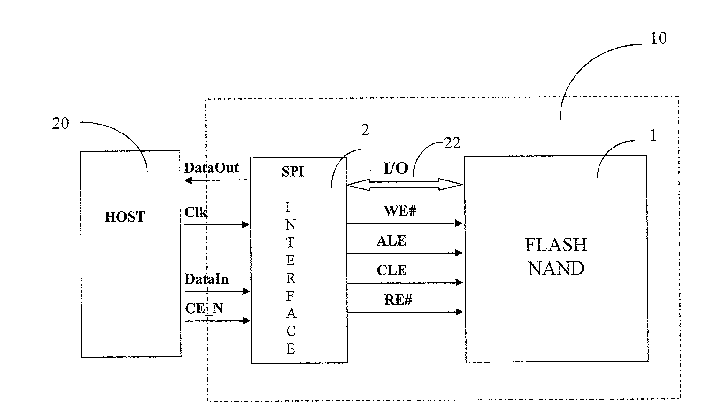
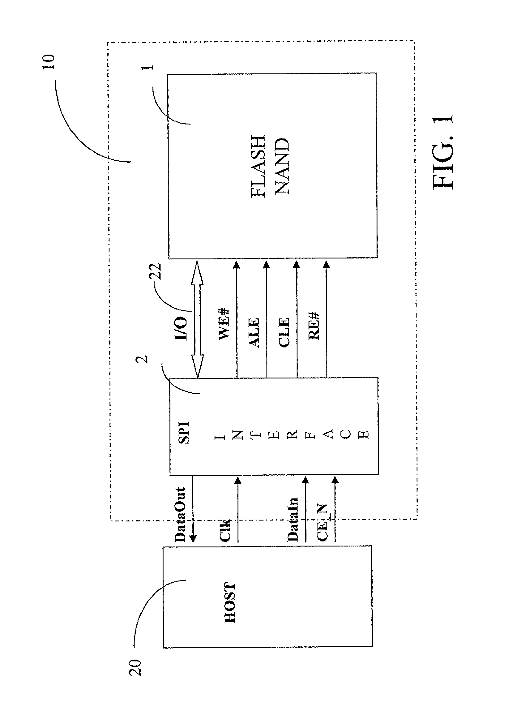
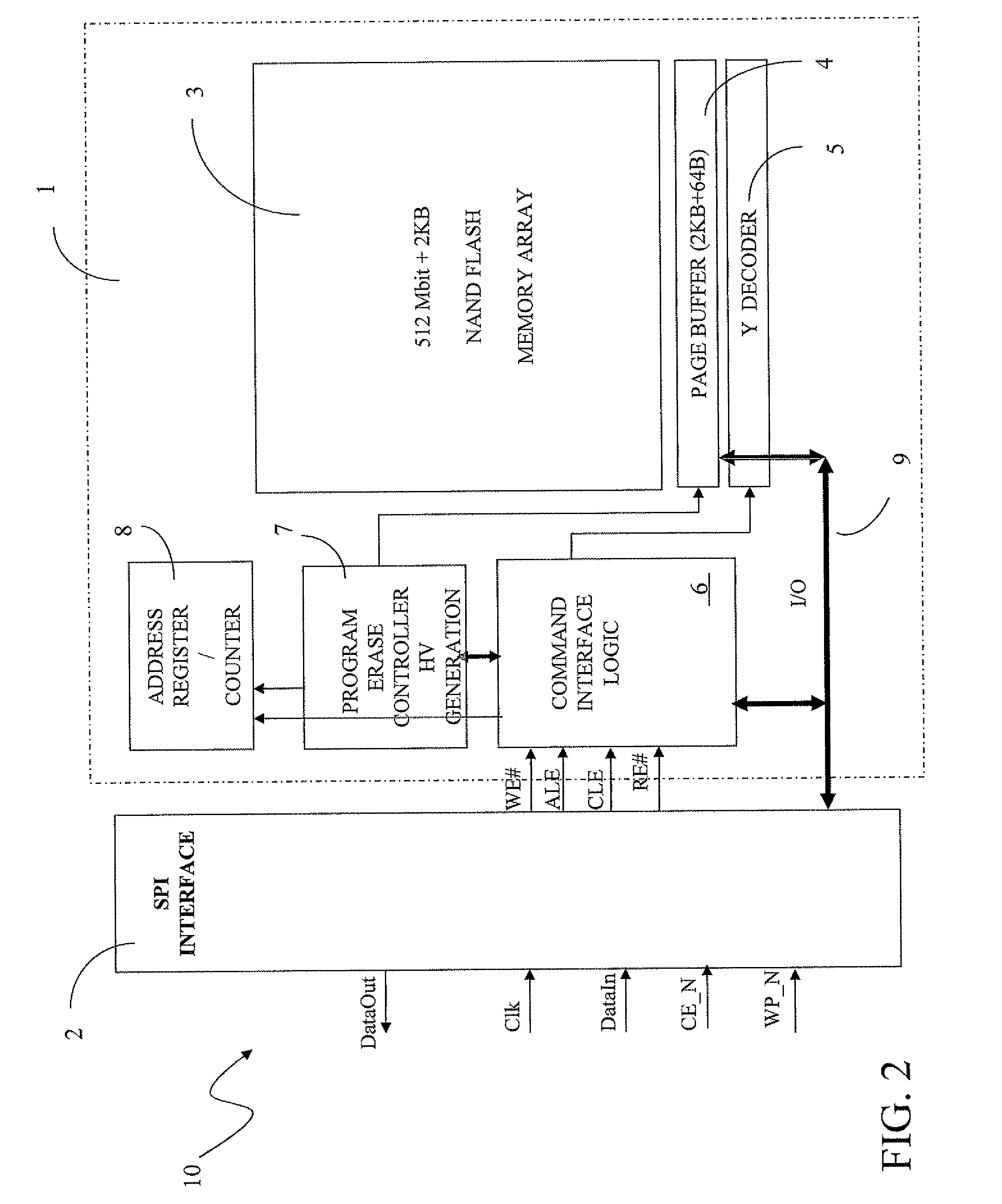
[0040] With reference to such figures, and in particular to FIG. 1, a memory architecture realized according to the present invention is illustrated and globally indicated with the reference number 10. In particular, the memory architecture 10 comprises a memory device 1 associated with an interface of the SPI type or SPI 2 in order to be connected to a host device 20. Advantageously, the memory device 1 is a Flash NAND memory.

[0041] In this way, the memory architecture 10 shows the following desired features: high density, fast erase and fast program. Moreover, as it will be clear from the following description, the SPI operations are based on a communication protocol which is completely independent from a Command Set of the memory device 1. In this way, if the memory device Command Set changes, the SPI 2 interface that connects the host device 20 remains the same.

[0042] The communication protocol supporting the SPI 2 is also completely independent from a size of the memory devic...


PUM


Abstract

A memory architecture includes a memory including a Command Set, and a serial peripheral interface (SPI) for connecting the memory to a generic host device. The SPI includes a data in line for supplying output data from the host device to inputs of the memory; a data out line for supplying output data from the memory to input of the host device; a clock line driven by the host device; and an enable line that allows the memory to be turned on and off by the host device. The memory is a NAND Flash Memory. The SPI includes an I/O registers block, including an SPI label register and a data register for driving separately data, commands and addresses directed to the memory from the corresponding SPI label registers.

Description

FIELD OF THE INVENTION [0001] The present invention relates to a memory architecture. More specifically, the invention relates to a memory architecture comprising a memory device, including a Command Set and a serial peripheral interface (SPI) for connecting the memory device to a generic host device. [0002] The invention also relates to a communication protocol for implementing the communication between a memory device connected to a host device through a serial peripheral interface (SPI). The invention particularly, but not exclusively, relates to a memory architecture of the Flash type and the following description is made with reference to this field of application for convenience of explanation only. BACKGROUND OF THE INVENTION [0003] A serial peripheral interface (SPI) is an interface that enables the serial (one bit at a time) exchange of data between two devices, one called a master and the other called a slave. An SPI operates in full duplex mode. This means that data can b...

Claims


Application Information

Patent Timeline
Patent Type & Authority Applications(United States)
IPC IPC(8): G11C7/00
CPCG06F13/4282G11C16/0483G11C16/08G11C16/26G11C2216/30
Inventor SARTORI, LAURACORSI, ADAMOROVEDA, MARCOLORUSSO, GIUSEPPE MAURIZIORUGGERI, DANIELAPELLICONE, DEMETRIO
Owner MICRON TECH INC
Why Eureka
Try Eureka