
Semiconductor intergrated circuit device

a technology of integrated circuits and semiconductors, applied in the direction of solid-state devices, fault locations, instruments, etc., can solve the problems of increasing the number of circuits, difficult to precisely execute testing when the difference exceeds an allowable value, and the loading required for designing can be significantly reduced, so as to achieve the effect of sufficient driving performance and easy design of large-scale circuits

Active Publication Date: 2007-06-07
SOCIONEXT INC
View PDF8 Cites 10 Cited by
  • Summary
  • Abstract
  • Description
  • Claims
  • Application Information

AI Technical Summary

Benefits of technology

[0007] The present invention is conceived of the aforementioned problems, and has an object to provide a semiconductor integrated circuit device capable of facilitating designing a large scale integrated circuit, particularly a system LSI designed with a combination of plural circuits using different IPs.
[0021] According to the semiconductor integrated circuit device of the present invention, it is possible to easily design a large-scale circuit, particularly a circuit of system LSI designed as a combination of circuits using plural IPs. Furthermore, testing efficiency can be improved, and a smaller semiconductor integrated circuit can be manufactured. In addition, signal input facility can be improved.

Problems solved by technology

Problems relating to circuit design such as timing design and the like are also found in addition to the aforementioned problem of the increase in the number of circuits.
Therefore, a clock phase difference is caused between flip-flops when test scanning, which is a known testing method for a large integrated circuit, is performed.
It is difficult to precisely execute testing when the difference exceeds an allowable value.
Accordingly, the circuit design cannot be easily realized because it is necessary to design timing considering the phase difference which occurs at the time of testing, when designing a semiconductor integrated circuit device as an integrated circuit.
Furthermore, the circuit design cannot be easily realized because, when the circuit is adjusted after being designed, only a single line for supplying a clock signal does not allow selecting and activating a local portion so as to evaluate the portion.

Method used


Image

  • Semiconductor intergrated circuit device
  • Semiconductor intergrated circuit device
  • Semiconductor intergrated circuit device

Examples


first embodiment

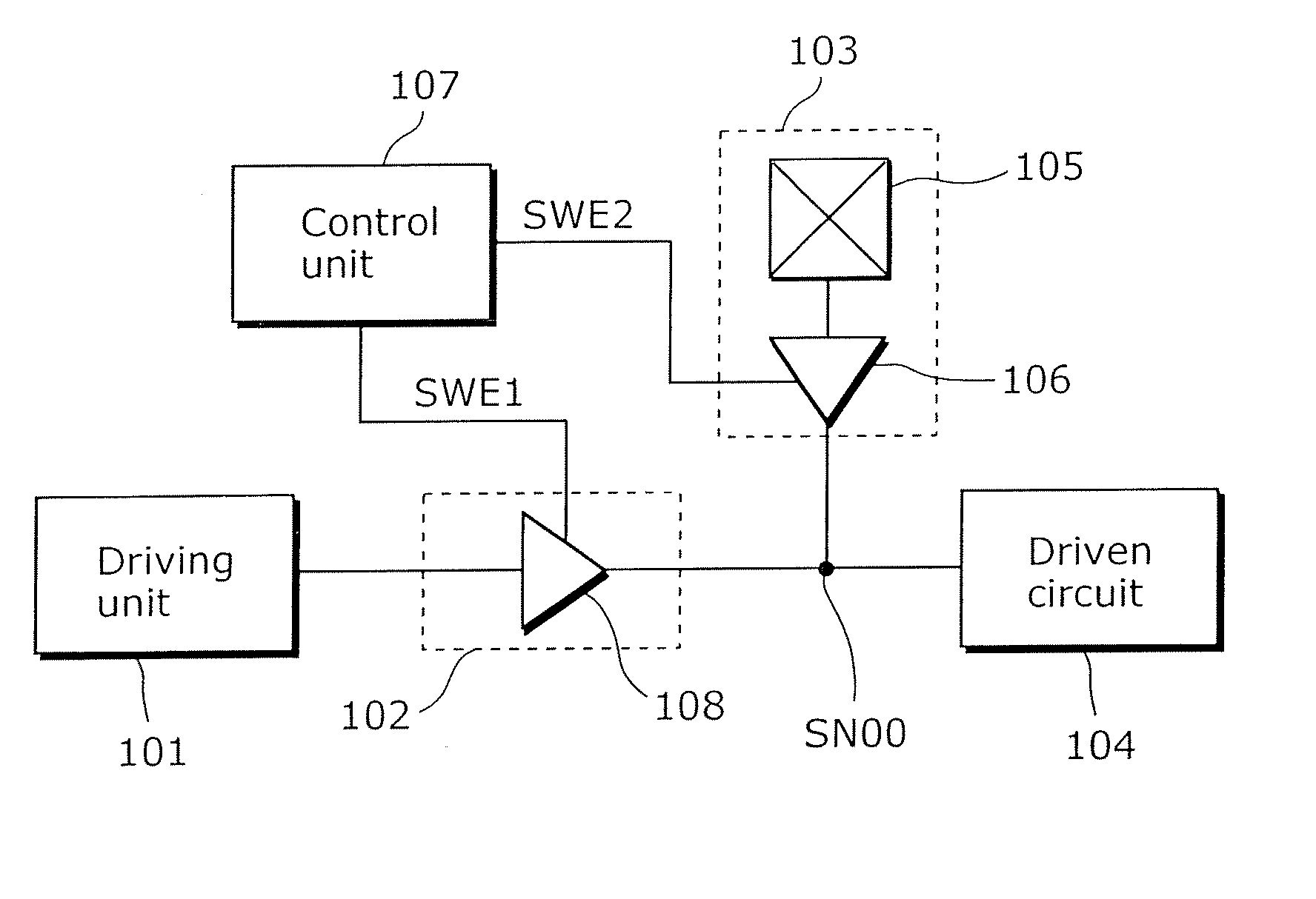
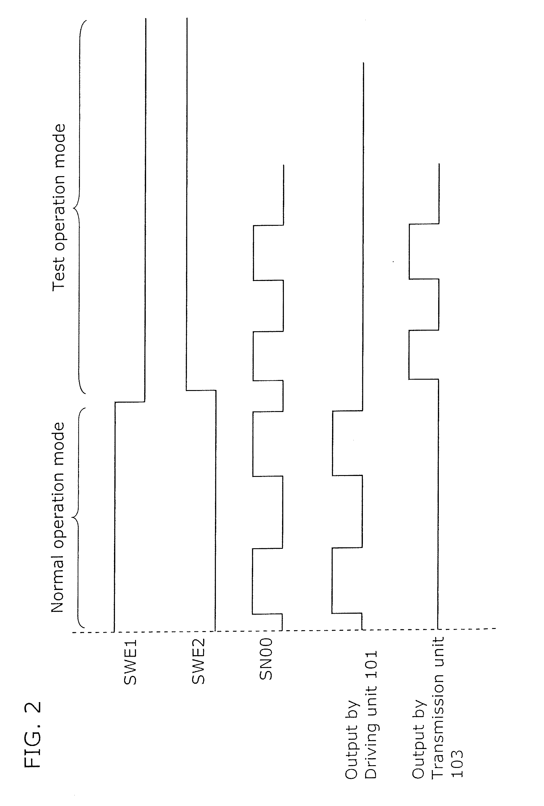
[0039]FIG. 1 is a diagram showing a schematic configuration of a semiconductor integrated circuit device according to the first embodiment of the present invention.

[0040] The semiconductor integrated circuit device includes a driving unit 101, a switch 102, a transmitting unit 103, a driven circuit 104, and a control unit 107. Note that, the driving unit 101, switch 102, transmitting unit 103, and control unit 107 are examples of a driving unit, a first switch, a transmitting unit, and a control unit of the present invention, respectively.

[0041] The driven circuit 104 is, for example, a circuit to be evaluated and adjusted, or a circuit including a flip-flop which performs a shift register operation at the time of scan testing.

[0042] The driving unit 101 is connected to the driven circuit 104 through a transmission line, receives a supply of a clock signal, generates a driving signal for driving the driven circuit 104, and supplies the driving signal to the driven circuit 104.

[0...

second embodiment

[0054]FIG. 3 is a diagram showing a schematic configuration of a semiconductor integrated circuit device according to the second embodiment of the present invention.

[0055] The semiconductor integrated circuit device includes a driving unit 101, a switch 102, a transmitting unit 303, a driven circuit 104, and a control unit 107. Note that, the transmitting unit 303 is an example of the transmitting unit of the present invention.

[0056] The transmitting unit 303 is connected to the transmission line between the switch 102 and the driven circuit 104, and transmits, to the driven circuit 104, the test signal supplied from outside the chip on which the semiconductor integrated circuit device is formed, instead of the driving signal. The transmitting unit 303 includes a capacitive coupled pad 305 which is connected to the outside by capacitive coupling, and into which the test signal is inputted from the outside, a receiver 307 which amplifies the test signal inputted via the capacitive ...

third embodiment

[0062]FIG. 5 is a diagram showing a schematic configuration of a semiconductor integrated circuit device according to the third embodiment of the present invention.

[0063] The semiconductor integrated circuit device includes a driving unit 101, a switch 102, a transmitting unit 503, a driven circuit 104, and a control unit 107. Note that, the transmitting unit 503 is an example of the transmitting unit of the present invention.

[0064] The transmitting unit 503 is connected to the transmission line between the switch 102 and the driven circuit 104, and transmits, to the driven circuit 104, a test signal supplied from outside the chip on which the semiconductor integrated circuit device is formed, instead of a driving signal. The transmitting unit 503 serves as an antenna, and is made up of an inductor 505 into which the test signal is externally inputted, and a tri-state buffer 506 which serves as a switch. The transmitting unit 503 directly drives the driven circuit 104 externally b...


PUM


Abstract

It is provided a semiconductor integrated circuit device capable of easily designing a large scale circuit, particularly a circuit of a system LSI designed by combining circuits using plural intellectual properties and the like. The semiconductor integrated circuit includes a driving unit which is connected to a driven circuit via a transmission line and supplies a driving signal for driving the driven circuit to the driven circuit, a switch which is inserted into the transmission line between the driven circuit and the driving unit and which causes the driving signal, which is to be supplied to the driven circuit, to flow or to be cut off, and a transmission unit which is connected to the transmission line between the switch and the driving unit, and which transmits, to the driven circuit, a test signal supplied from outside the semiconductor integrated circuit device instead of the driving signal.

Description

BACKGROUND OF THE INVENTION [0001] (1) Field of the Invention [0002] The present invention relates to an evaluation and adjustment method of a semiconductor integrated circuit device, and particularly to an evaluation method of a System Large Scale Integration (LSI) which is designed based on Intellectual Property (IP). [0003] (2) Description of the Related Art [0004] It has been possible to manufacture a large scale integrated circuit onto one semiconductor chip by integrating complicated systems onto the semiconductor chip, following the dramatic increase in the number of transistors which can be integrated onto one semiconductor chip due to fine processing (for example, Patent Reference 1: Japanese Laid-Open Patent Application No. 2002-533738). Furthermore, the number of circuits, which do not contribute to normal operations of a Super Large Scale Integration (SLSI) such as test circuits and timing adjustment circuits, has been increased in order to test such large scale integrat...

Claims


Application Information

Patent Timeline
Patent Type & Authority Applications(United States)
IPC IPC(8): G01R31/08
CPCG01R31/312G01R31/315G01R31/31713G01R31/318533H01L2924/0002H01L2924/00
Inventor TANAKA, ISAO
Owner SOCIONEXT INC
Features
  • Generate Ideas
  • Intellectual Property
  • Life Sciences
  • Materials
  • Tech Scout
  • Unparalleled Data Quality
  • Higher Quality Content
  • 60% Fewer Hallucinations
Learn More