Switching power supply capable of reducing low-frequency secondary-side common-mode voltage
- Summary
- Abstract
- Description
- Claims
- Application Information
AI Technical Summary
Benefits of technology
Problems solved by technology
Method used
Image
Examples
Embodiment Construction
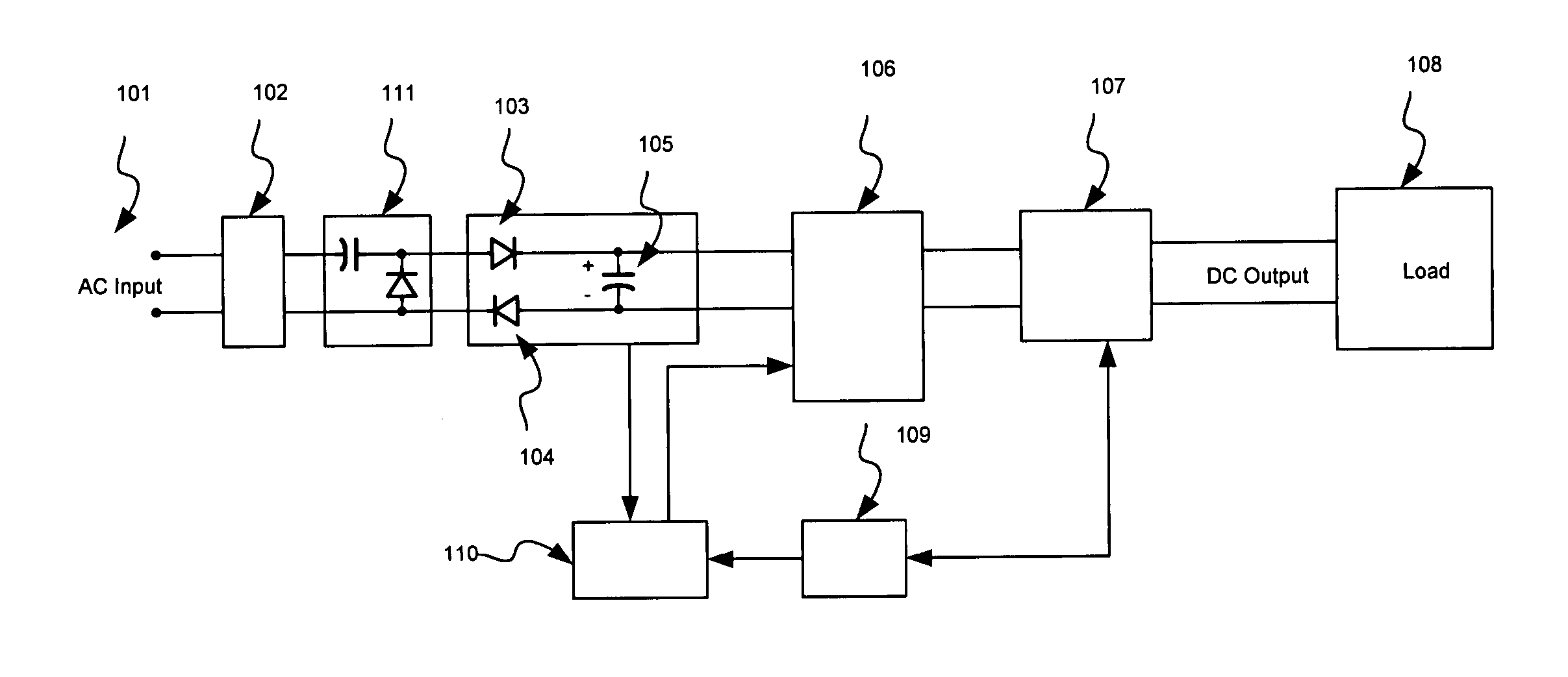
[0024]FIG. 6 is block diagram showing a switching power supply capable of reducing a low-frequency secondary-side common-mode voltage according to an embodiment of the invention. Referring to the FIG. 6, the power supply 1 includes an input filtering device 102, a first common-mode filtering circuit device 103, a second common-mode filtering circuit device 104, a filtering capacitor 105, a transformer & switch device 106, an output filter & voltage regulator 107, a photo coupler 109 and a PWM and control circuit 110. When the input voltage is at the positive half cycle, the current flows through the first common-mode filtering circuit device 103 to charge the filtering capacitor 105 and then flows back to a power source from the second common-mode filtering circuit device 104. At this moment, the low-frequency common mode voltage with the positive half cycle still exists. When the input voltage is at the negative half cycle, the input voltage is blocked using the second common-mode ...
PUM
 Abstract
Description
Claims
Application Information


