

Process and apparatus for forming oxide film, and electronic device material
a technology of forming oxide film and electronic devices, which is applied in the direction of coatings, chemical vapor deposition coatings, electric discharge tubes, etc., can solve the problems of affecting the fabrication of finer devices, thermal oxidation process still requires a temperature of about 800° c. or higher, and impurity again dispersed
- Summary
- Abstract
- Description
- Claims
- Application Information
AI Technical Summary
Benefits of technology
Problems solved by technology
Method used
Image

Examples
embodiment of
One Embodiment of Production Process
[0096] Next, there is described an embodiment of the oxide film-forming process according to the present invention.
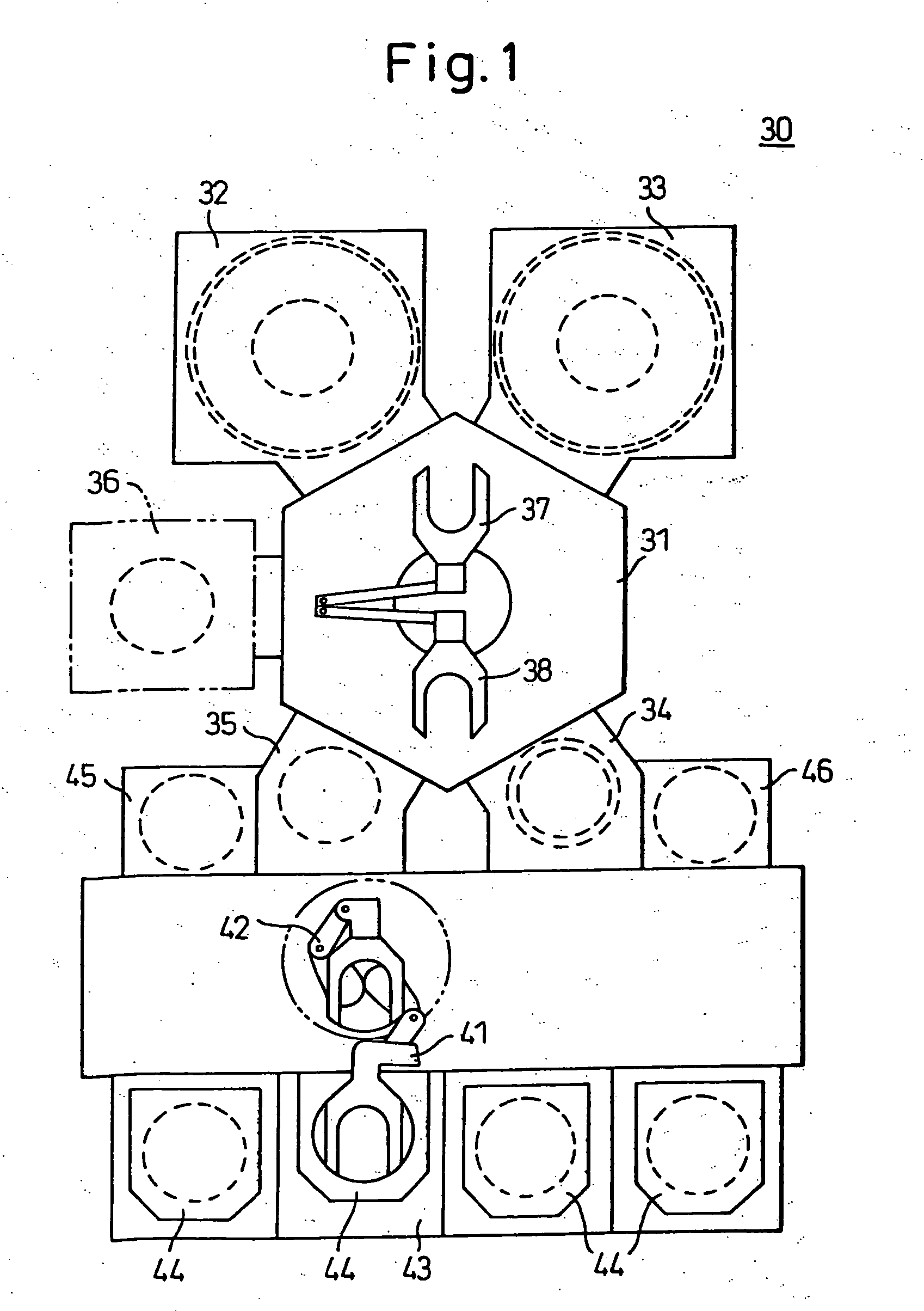
[0097]FIG. 1 is a schematic view (schematic plan view) showing an example of the total arrangement of a semiconductor manufacturing equipment 30 for conducting the oxide film-forming process according to the present invention.
[0098] As shown in FIG. 1, in a substantially central portion of the semiconductor manufacturing equipment 30, there is disposed a transportation chamber 31 for transporting a wafer W (FIG. 3). Around the transportation chamber 31, there are disposed: plasma processing units 32 and 33 for conducting various treatments on the wafer, two load lock units 34 and 35 for conducting the communication / cutoff between the respective processing chambers, a heating unit 36 for operating various heating treatments, and a heating reaction furnace 47 for conducting various heating treatments on the wafer. These units are disp...
example 1
[0165] (Oxide Film Formation)
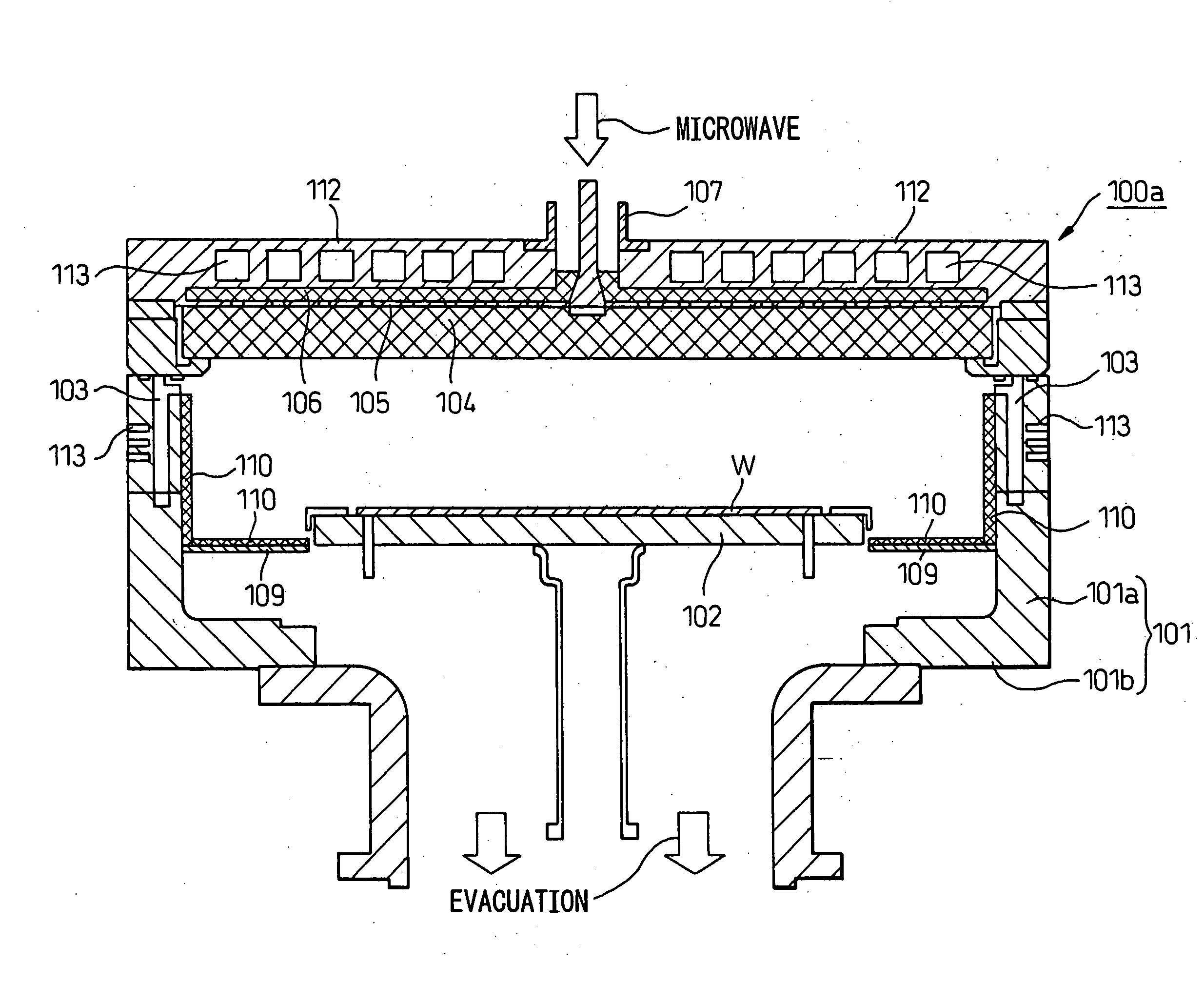
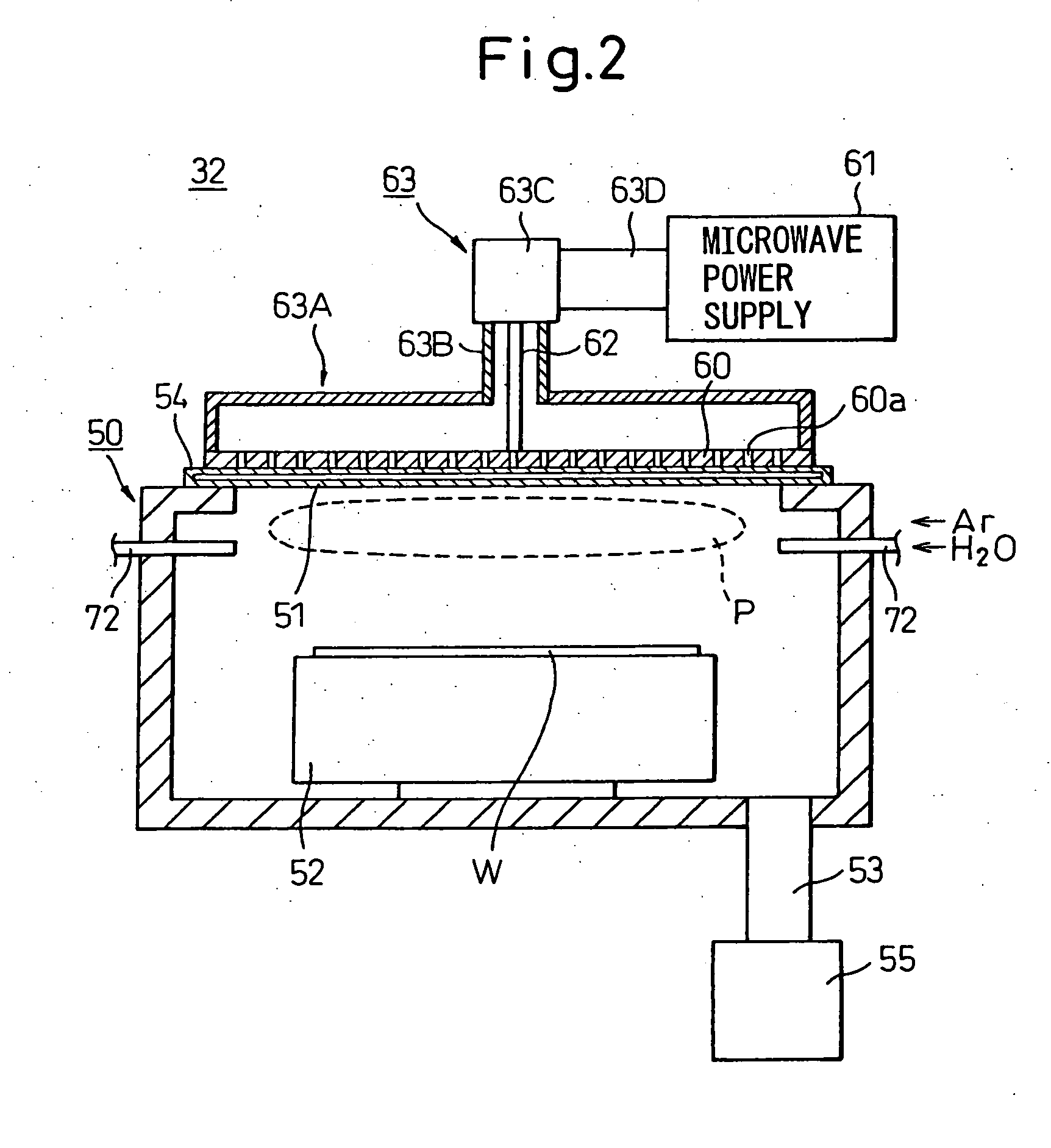
[0166] An oxide film was formed on a silicon substrate by the oxide film-forming process according to the present invention. In the formation of this oxide film, a process chamber having a plane antenna member as shown in FIG. 1 and FIGS. 11-12 was used.
[0167] (Substrate)
[0168] As a silicon substrate, a monocrystalline silicon substrate (wafer) having a specific resistance of 8 (cm, a P type of a diameter of 200 mm and a plane orientation (100) was used.
[0169] (Prewashing)
[0170] The silicon substrate was washed in the following procedure. [0171] 1. Immerse in hyperammonium aqueous solution (10 minutes) [0172] 2. Rinse in pure water [0173] 3. Immerse in hyperhydrochloric acid aqueous solution (10 minutes) [0174] 4. Rinse in pure water [0175] 5. Immerse in hyperhydrofluoric acid aqueous solution (8 minutes) [0176] 6. Rinse in pure water [0177] 7. Dry in nitrogen gas
[0178] (Plasma Oxidation Treatment)
[0179] Microwave output: 3500 W
[0180] Chamber pre...
example 2
Measurement of Dependence on Crystal Orientation
[0186] Using a silicon substrate wherein trench groove had previously been processed, the same prewashing and plasma processing as Example 1 was carried out.
[0187] The dependence on crystal orientation of oxide film thickness was determined by the TEM observation of the cross section of the oxide film of trench groove. The result of measurement is shown in TEM photographs in the following (Table 1) and FIG. 16.
TABLE 1CrystalRatio ofPositionFilm thicknessorientationfilm thickness12001001.0021901.0532301100.8741701.1852001001.00
PUM
| Property | Measurement | Unit |
|---|---|---|
| temperature | aaaaa | aaaaa |
| pressure | aaaaa | aaaaa |
| temperature | aaaaa | aaaaa |
Abstract
Description
Claims
Application Information