
Spin-on glass passivation process

a spin-on glass and passivation technology, applied in the direction of basic electric elements, semiconductor/solid-state device manufacturing, electric apparatus, etc., can solve the problems of increasing the power consumption of the ic, increasing the rc time constant, and reducing signal propagation speed, so as to reduce or eliminate the migration of moisture or mobile ions, the effect of enhancing chemical vapor deposition

Inactive Publication Date: 2007-06-07
MACRONIX INT CO LTD
View PDF5 Cites 0 Cited by
  • Summary
  • Abstract
  • Description
  • Claims
  • Application Information

AI Technical Summary

Benefits of technology

[0010] Any composition or material suitable as a barrier layer is envisioned as the first barrier layer. Preferred barrier layers are capable of reducing or eliminating the migration of moisture or mobile ions. In some embodiments, the first barrier layer is a silicon oxynitride or silicon nitride layer. Silicon nitride or silicon oxynitride layers formed to provide a compressive force maybe particularly useful in certain embodiments. Plasma enhanced chemical vapor deposition (CVD) or other process can be used to provide suitable barrier layers.
[0012] Any composition or material suitable as a barrier layer is envisioned as the second barrier layer. The second barrier layer is formed to provide a compressive force. Some such layers are also capable of reducing or eliminating the migration of moisture or mobile ions. In some embodiments, the second barrier layer is a silicon oxynitride or silicon nitride layer. Plasma enhanced chemical vapor deposition (CVD) or other process can be used to provide suitable barrier layers.

Problems solved by technology

The increased capacitance further results in increased power consumption for the IC and an increased RC time constant, the latter resulting in reduced signal propagation speed.
In sum, the effects of miniaturization cause increased power consumption, limit achievable signal speed, and degrade noise margins used to insure proper IC device or chip operation.
Many dielectric materials have been proposed for use as dielectric film coatings in semi-conductor devices, but most of them are considered to be unsatisfactory in meeting the stringent electrical and physical requirements.
The preferred formation of these inorganic dielectrics by chemical vapor deposition processes leaves these inorganic dielectric layers inherently uneven because plasma based deposition processes exactly reproduce the uneven and stepped profile structure of the underlying wiring pattern.
However, such materials are typically less desirable due to poor thermal stability or poor adhesion characteristics.

Method used


Image

  • Spin-on glass passivation process
  • Spin-on glass passivation process
  • Spin-on glass passivation process

Examples


Embodiment Construction

.”

BRIEF DESCRIPTION OF THE DRAWINGS

[0015] Features, aspects, and embodiments of the inventions are described in conjunction with the attached drawings, in which:

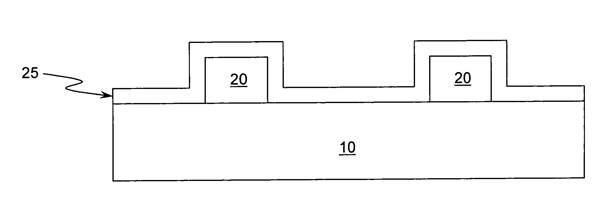
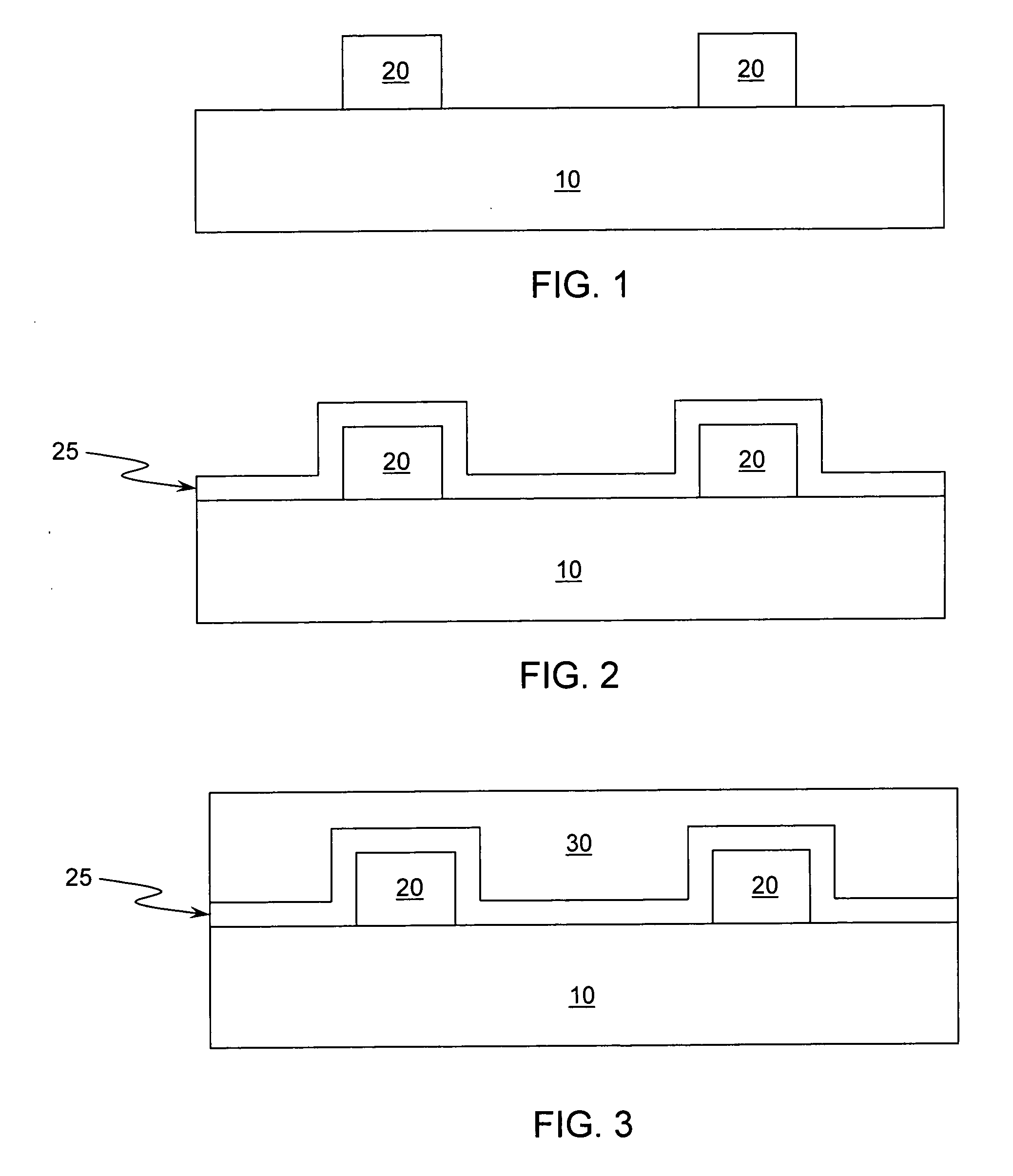
[0016]FIG. 1 illustrates an embodiment of a semiconductor device having a substrate with device or isolation features formed thereon at an intermediate stage of production;

[0017]FIG. 2 illustrates an embodiment of a semiconductor device having a barrier layer formed over the substrate and device or isolation features at an intermediate stage of production;

[0018]FIG. 3 illustrates an embodiment of a semiconductor device having an insulating spin-on glass layer formed over the barrier layer, the device or isolation structures, and the substrate at an intermediate stage of production; and;

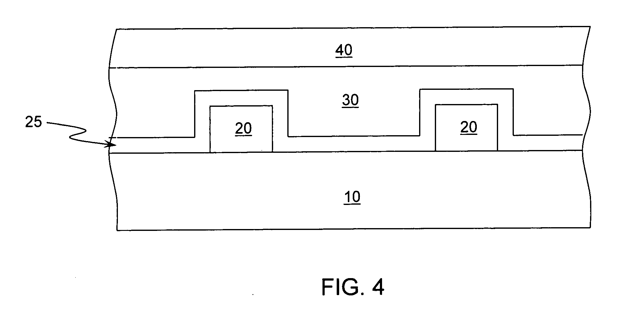
[0019]FIG. 4 illustrates an embodiment of the invention after deposition of the compressive barrier layer over the insulating spin-on glass layer, the barrier layer, the device or isolation structures, and the substrate.

DETAILED DESCRIPTI...


PUM


Abstract

Integrated circuits and methods of making an integrated circuit are disclosed. The disclosed methods include providing a substrate having at least one device structure thereon; providing a first barrier layer over the substrate and the at least one device structure; providing a dielectric layer formed by a spin-on-glass process; and providing a second barrier layer over the dielectric layer, wherein the second barrier layer is a compressive layer. Integrated circuits described herein include a first barrier layer over the substrate and the at least one device structure; a dielectric layer formed by a spin-on-glass process; and a second barrier layer over the dielectric layer, wherein the second barrier layer is a compressive layer.

Description

BACKGROUND [0001] 1. Field of the Invention [0002] Embodiments of the invention relate to methods for passivating spin-on-glass layers of semiconductor wafers and wafers and devices made therefrom. [0003] 2. Background of the Invention [0004] In the prior art production of semiconductor integrated circuit devices, fine patterns of semiconductor regions, electrodes, wiring and other components are fabricated onto the semiconductor substrate by using conventional process steps, one being chemical vapor deposition (CVD). After formation of the wire pattern on the device, an interline dielectric material deposition is formed between the horizontally disposed wiring, the pattern overlaid with dielectric film forming material, and multi-layer formation processes, well-known in the art, are provided to form a multi-layered integrated semiconductor device. [0005] Presently, advances in the semiconductor industry are characterized by the introduction of new generations of integrated circuits...

Claims


Application Information

Patent Timeline
Patent Type & Authority Applications(United States)
IPC IPC(8): H01L21/31
CPCH01L21/02126H01L21/02216H01L21/02282H01L21/02304H01L21/02362H01L21/3122H01L21/316H01L21/76801H01L21/76829H01L21/76834
Inventor CHEN, LEE-JENSU, CHIN-TA
Owner MACRONIX INT CO LTD
Learn More