

Optical integrator, illumination optical device, exposure device, and exposure method
a technology of optical integrator and illumination optical device, which is applied in the direction of photomechanical equipment, instruments, printers, etc., can solve the problems of not having optically transparent materials available, unable to increase, and need to further reduce the wavelength of exposure light, so as to reduce the reflectance of reflecting films, suppress aberration, and avoid interference
- Summary
- Abstract
- Description
- Claims
- Application Information
AI Technical Summary
Benefits of technology
Problems solved by technology
Method used
Image

Examples
first embodiment
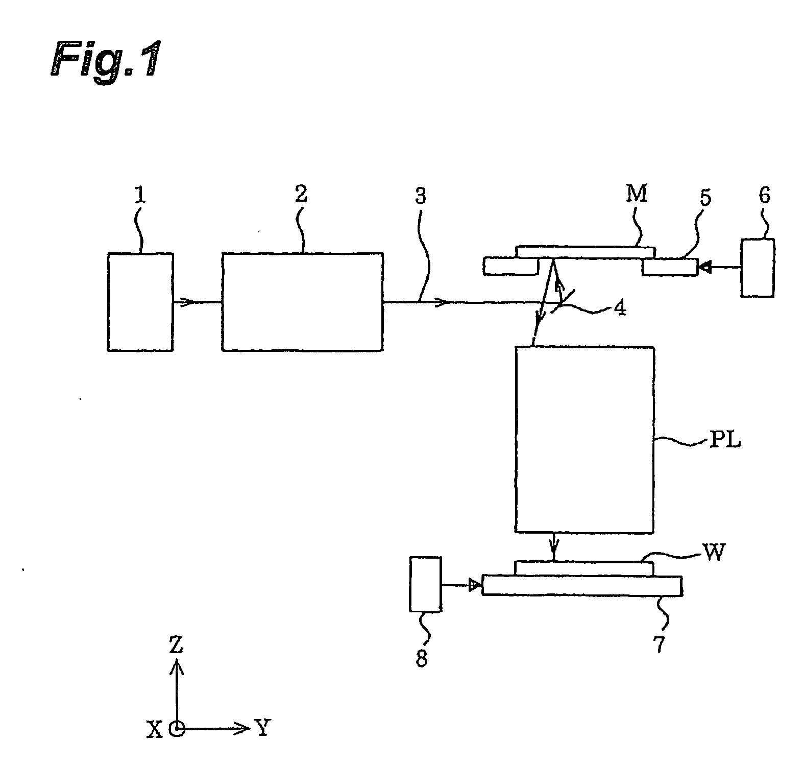
[0048] Referring to FIG. 1, the exposure apparatus of the first embodiment has a light source for supplying exposure light, e.g., a laser plasma light source 1. Light emitted from the light source 1 is guided through a wavelength-selecting filter (not shown) to enter an illumination optical system 2. The wavelength-selecting filter herein has such characteristics as to selectively transmit only EUV light of a predetermined wavelength (e.g., 13.4 nm or 11.5 nm) and to interrupt light of the other wavelengths out of the light supplied from the light source 1. The EUV light 3 having passed through the wavelength-selecting filter travels via the illumination optical system 2 and a plane reflecting mirror 4 as a path deflector to illuminate a reflective mask (reticle) M in which a pattern to be transferred is formed.
[0049] The mask M is held by a mask stage 5, which is movable along the Y-direction, so that a pattern surface thereof extends along the XY plane. A laser interferometer 6 is...
second embodiment
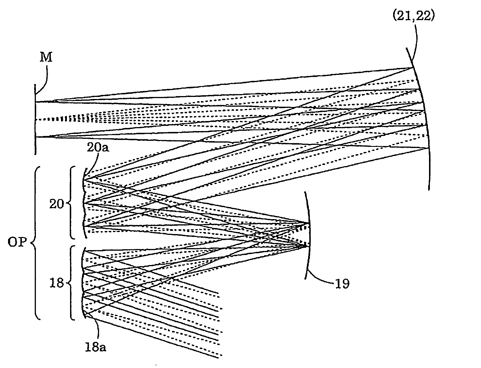
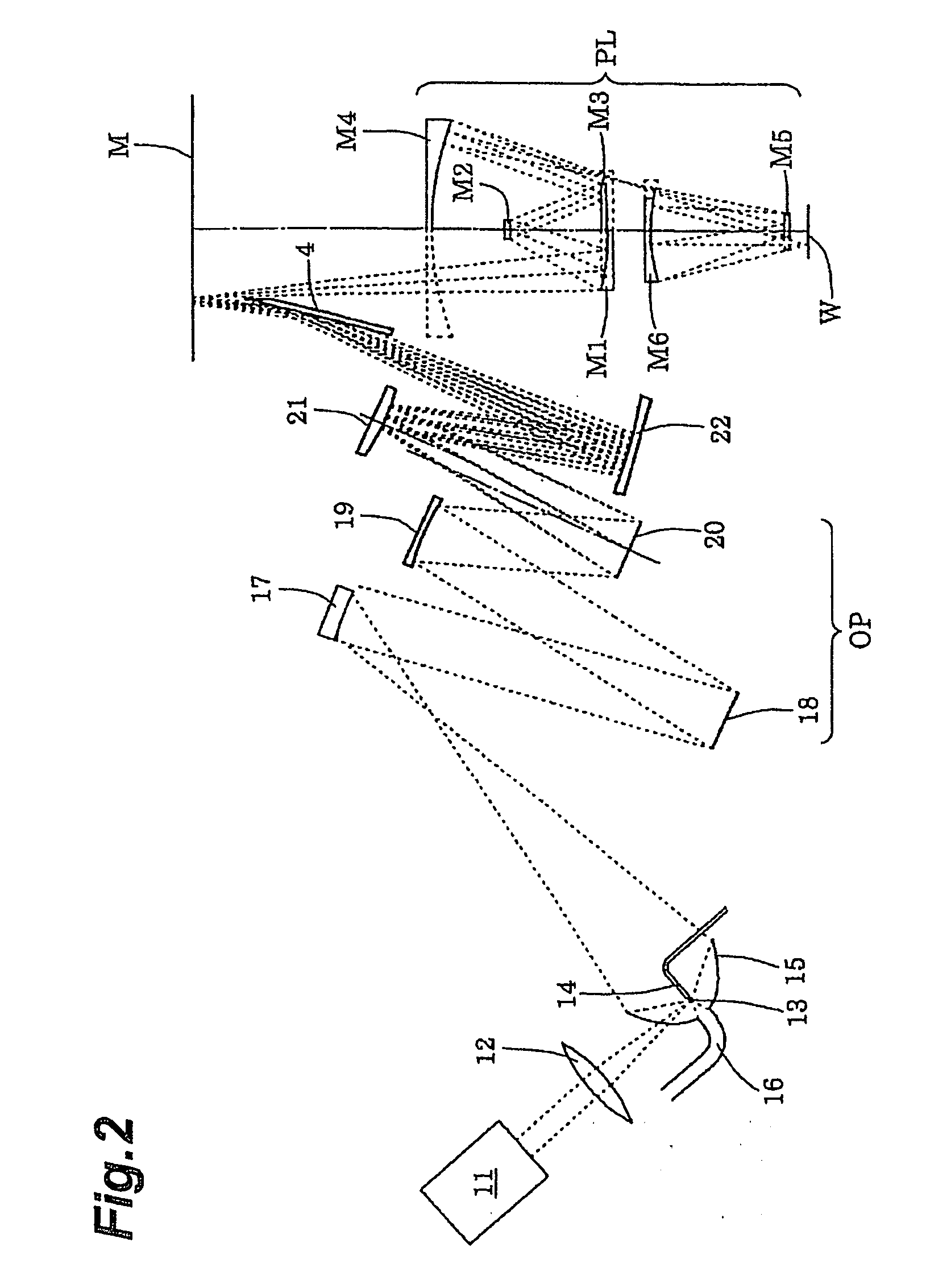
[0071] In the first fly eye mirror 18, the first concave reflector elements 18a need to be arranged in parallel by an enough number both in the horizontal direction and in the vertical direction, in order to achieve the required wavefront dividing effect. For this reason, if the outer shape of the first concave reflector elements 18a is set to the oblong arcuate shape similar to the outer shape of the static exposure region ER of the wafer W as in the conventional technology, the number of first concave reflector elements arranged along the transverse direction of the outer shape will become too large (cf. FIG. 12(b) for the second embodiment described later), which will adversely affect the production cost of the first fly eye mirror 18 and, in turn, the production cost of the optical integrator OP.
[0072] In the first embodiment, as described above, each of the first concave reflector elements 18a, the second concave reflector elements 20a, and the concave reflecting mirror 19 is c...
PUM
 Abstract
Description
Claims
Application Information