Light scattering layer for electronic device comprising nano-particles, junction structure for thin film transistor comprising light scattering layer, and methods of forming the same

a technology of nano-particles and junction structures, applied in semiconductor devices, instruments, chemistry apparatuses and processes, etc., can solve the problems of difficult to reproduce regular junctions in josephsen junctions, difficult to consistently manufacture a number of junctions, and difficult to use in manufacturing integrated circuits. achieve the effect of thin film transistors and reducing the total thickness of junction structures

Inactive Publication Date: 2007-06-14
ELECTRONICS & TELECOMM RES INST
View PDF4 Cites 5 Cited by
  • Summary
  • Abstract
  • Description
  • Claims
  • Application Information

AI Technical Summary

Benefits of technology

[0021] In accordance with the present invention, a miniaturized and integrated electronic device is realized by using the light scattering layer including the carbide-semimetal or carbide-metal, i.e., (MC)1-xMx (wherein, M is Si, Ta, W or Mo, and 0<x<1). For this purpose, a three-layer structure is formed by including the protective layer-light scattering layer-protective layer, or a five-layer structure is formed by including the protective layer-capping layer-light scattering layer-capping layer-protective layer are formed, thereby making it easy to generate the nano-partic

Problems solved by technology

This is severely disadvantageous when manufacturing electronic devices which place a large emphasis on miniaturization.
However, since the YBCO thin film is sensitive to oxygen doping due to its composite oxide structure, it is difficult to consistently manufacture a number of junctions and it is also difficult to us

Method used


Image

  • Light scattering layer for electronic device comprising nano-particles, junction structure for thin film transistor comprising light scattering layer, and methods of forming the same
  • Light scattering layer for electronic device comprising nano-particles, junction structure for thin film transistor comprising light scattering layer, and methods of forming the same
  • Light scattering layer for electronic device comprising nano-particles, junction structure for thin film transistor comprising light scattering layer, and methods of forming the same

Examples


Embodiment Construction

[0024] The present invention will now be described more fully hereinafter with reference to the accompanying drawings, in which preferred embodiments of the invention are shown.

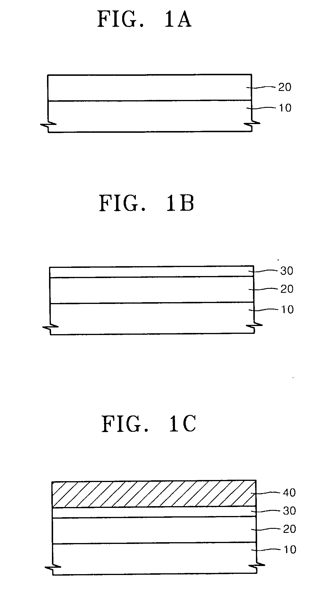
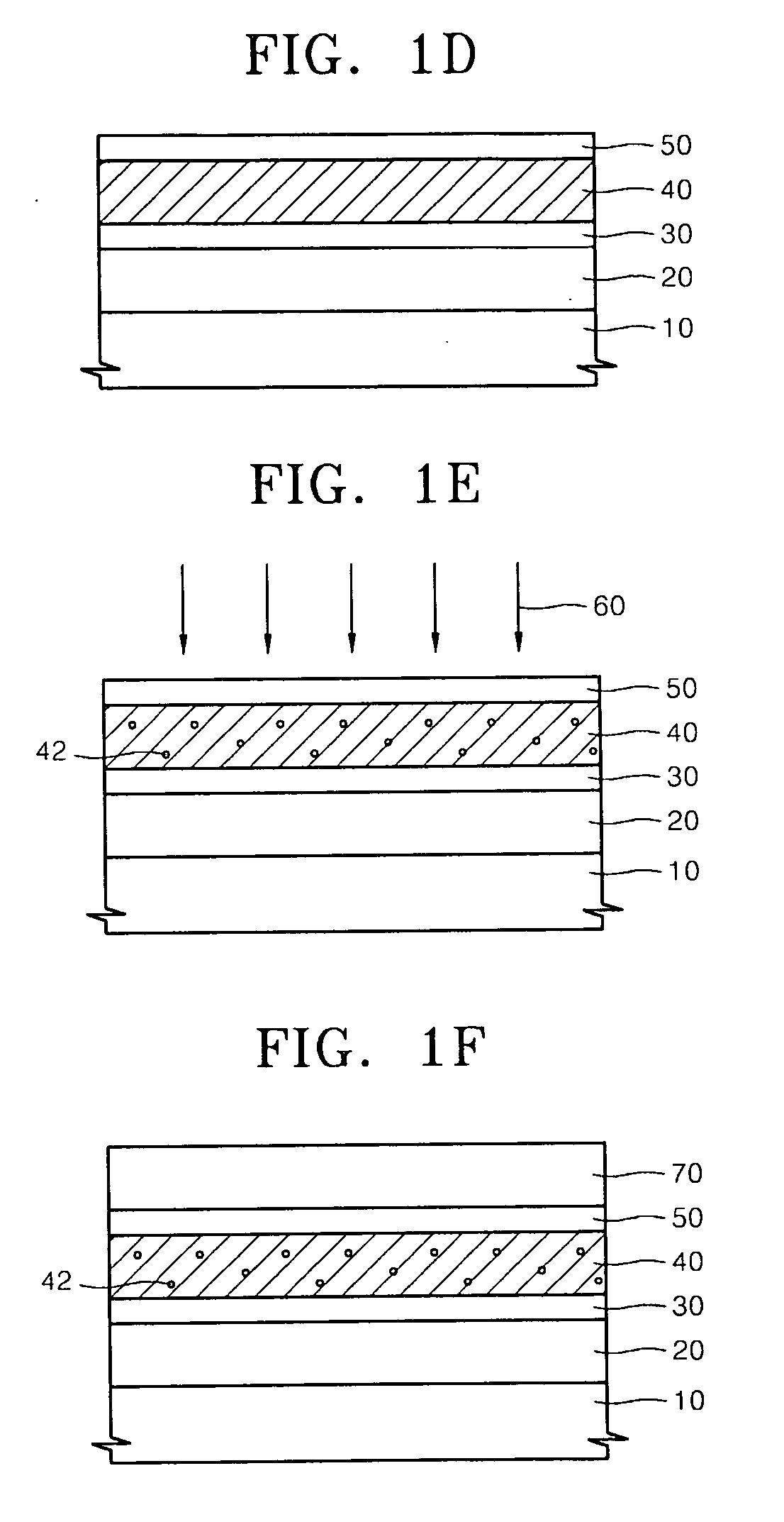
[0025]FIGS. 1A through 1G are cross-sectional views illustrating a method of forming a junction structure for a thin film transistor comprising a light scattering layer which can be used in an electronic device according to an embodiment of the present invention.

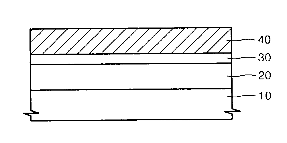
[0026] Referring to FIG. 1A, a substrate 10 comprises any one selected from the group consisting of GaN, Al2O3, SiC, ZnO, LiAlO2, LiGaO2, MgO, and SrTiO3, or a combination thereof.

[0027] A first protective layer 20 is formed on the substrate 10. The first protective layer 20 comprises a carbide and is formed to a thickness of about 10˜300 nm. The first protective layer 20 comprises at least one carbide selected from the group consisting of (ZnS)1-x(SiC)x, W1-xCx, Ta1-xCx, and Mo1-Cx (wherein, 0

[0028] Referring to FIG. 1B, a fir...


PUM

PropertyMeasurementUnit
Temperatureaaaaaaaaaa
Thicknessaaaaaaaaaa

Abstract

A light scattering layer for an electronic device comprising nano-particles, a junction structure for a thin film transistor comprising the light scattering layer, and methods of forming the same are provided. The light scattering layer for the electronic device comprises a carbide-semimetal or a carbide-metal comprising nano-particles comprising Si or a metal. In the junction structure for a thin film transistor according to an embodiment of the present invention, the light scattering layer is interposed between a first protective layer and a second protective layer comprising (ZnS)1-x(SiC)x, W1-xCx, Ta1-xCx, and Mo1-xCx, wherein 0<x<1. First and second capping layers comprising M1-y((ZnS)1-x(SiC)x)y, M1-y(W1-xCx)y, M1-y(Ta1-xCx)y, and M1-y(Mo1-xCx)y, wherein 0<x<1, 0<y<1, and M is Si, Ta, W or Mo, may be interposed between the first protective layer and the light scattering layer, and between the light scattering layer and the second protective layer, respectively. The layers are sequentially formed in-situ, without breaking a vacuum state after the process of forming each layer is performed.

Description

CROSS-REFERENCE TO RELATED PATENT APPLICATION [0001] This application claims the benefits of Korean Patent Application No. 10-2005-0119474, filed on Dec. 8, 2005, and Korean Patent Application No. 10-2006-0030508, filed on Apr. 4, 2006, in the Korean Intellectual Property Office, the disclosures of which are incorporated herein in its entirety by reference. BACKGROUND OF THE INVENTION [0002] 1. Field of the Invention [0003] The present invention relates to a light scattering layer for an electronic device, an electric junction structure including the light scattering layer, and methods of forming the same, and more particularly, to a light scattering layer for an electronic device comprising nano-particles, a junction structure for a thin film transistor consisting of a protective layer-a light scattering layer-a protective layer structure, and methods of forming the same. [0004] 2. Description of the Related Art [0005] Conventional thin film transistor devices use a technique of am...

Claims


Application Information

Patent Timeline
IPC IPC(8): B32B9/00
CPCG02B5/0242H01L29/78633H01L33/22
Inventor KIM, SANG HYEOB
Owner ELECTRONICS & TELECOMM RES INST
Why Eureka
Try Eureka