Plasma processing apparatus

a processing apparatus and plasma technology, applied in plasma technology, energy-based chemical/physical/physico-chemical processes, coatings, etc., can solve problems such as circuit element defects and plasma surface damage, and achieve the effect of preventing damage to the wafer

Inactive Publication Date: 2007-06-21
TOKYO ELECTRON LTD
View PDF2 Cites 81 Cited by
  • Summary
  • Abstract
  • Description
  • Claims
  • Application Information

AI Technical Summary

Benefits of technology

[0009] Accordingly, the object of the present invention is to provide a plasma processing apparatus capable of utilizing a generated radical effectively, while preventing damage to the wafers.
[0010] A further object of the present invention is to suppress hollow cathode discharge and sputtering due to plasma.
[0015] In a preferred embodiment, the plasma gas nozzle is arranged at a position remote from a plasma generating area between the plasma electrodes at a distance enough large to prevent generation of hollow cathode discharge.

Problems solved by technology

That is, in the plasma processing apparatus of FIG. 9, as the wafers W are directly exposed to a plasma, the plasma may seriously damage the wafer surfaces.
Further, as the gas nozzle 10 made of quartz is located in an electric field generated between the electrodes 4 and 6, the gas nozzle 10 is sputtered by a plasma to generate particles, resulting in defects in circuit elements.
Moreover, impurities decomposed by the sputter are introduced into deposition films on the wafers W. Further, as a large pressure difference exists near the gas holes 10A of a small diameter through which a plasma gas or a process gas is supplied, so-called “hollow cathode discharge” is generated, and thus the quartz gas nozzle 10 is sputtered, resulting in the same problem as mentioned above.

Method used


Image

  • Plasma processing apparatus
  • Plasma processing apparatus
  • Plasma processing apparatus

Examples


Embodiment Construction

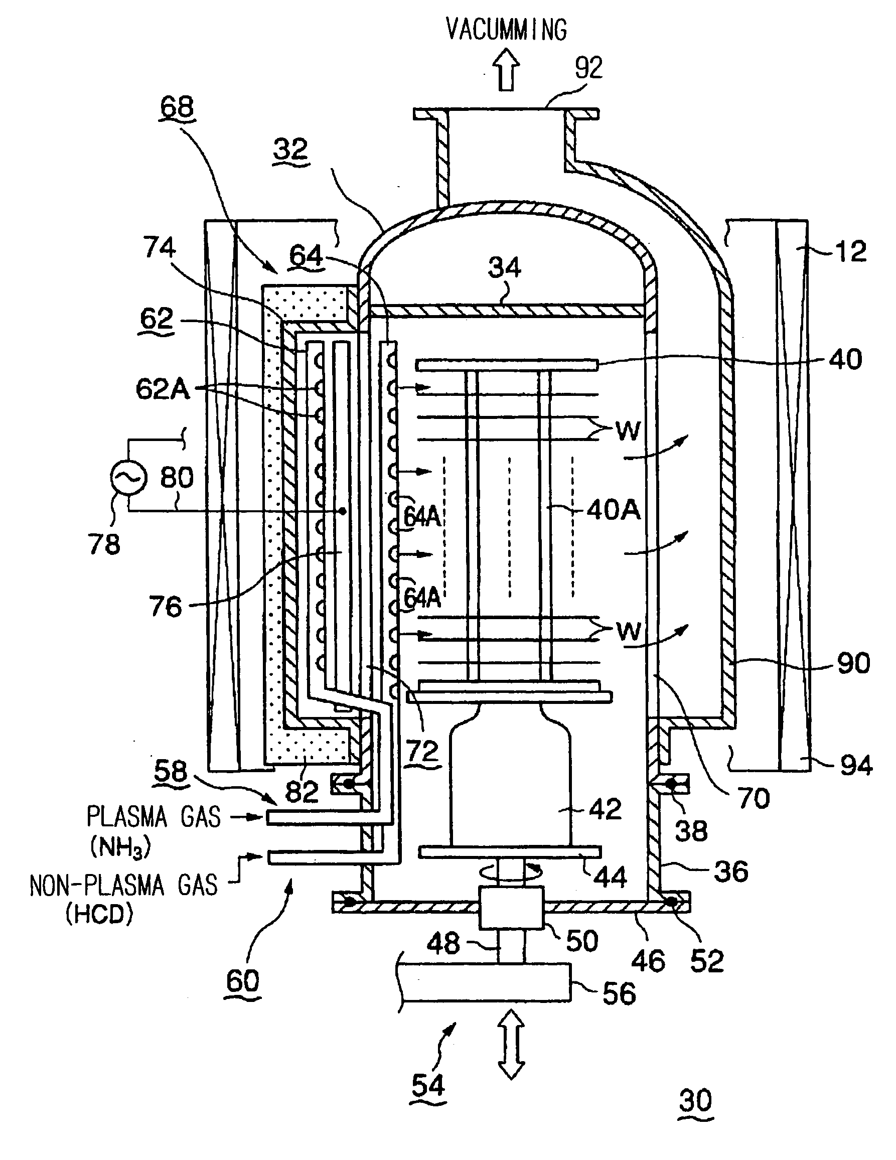
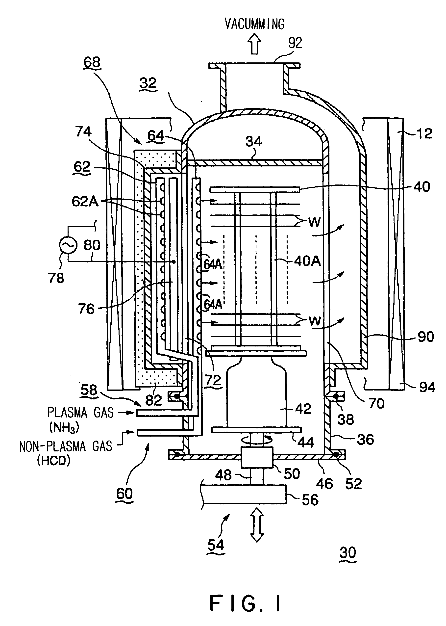
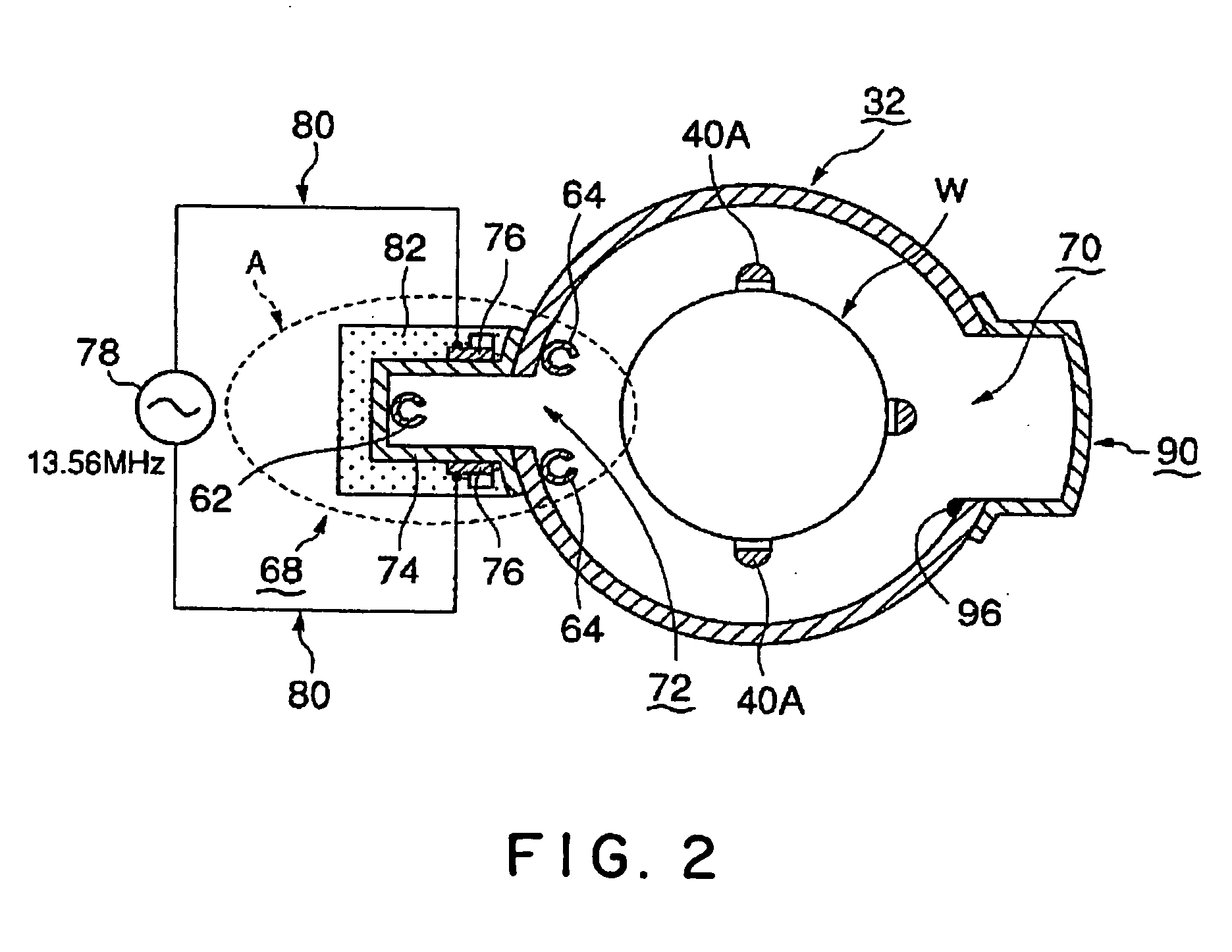
[0030] A plasma processing apparatus in one embodiment of the present invention is described in detail below with reference to the accompanying drawings. FIG. 1 is a vertical sectional view of the plasma processing apparatus. FIG. 2 is a transverse sectional view of the plasma processing apparatus (illustration of a heater is omitted). FIG. 3 is an enlarged view of a part A in FIG. 2. FIG. 4 is a perspective view showing the arrangement of plasma electrodes. FIG. 5 is a timing diagram showing the process gas supply timing. Hereinbelow, a film forming process for forming a silicon nitride (SiN) film by a plasma assisted chemical vapor deposition is described by way of example, with the use of ammonia gas as a gas to be converted into a plasma (referred to as “plasma gas” below) and hexachlorodisilane (also referred to as “HCD” below) gas as a gas not to be converted into a plasma (referred to as “non-plasma gas” below).

[0031] The plasma processing apparatus 30 includes a cylindrical...


PUM

PropertyMeasurementUnit
diameteraaaaaaaaaa
diameteraaaaaaaaaa
frequencyaaaaaaaaaa

Abstract

The invention is intended, in a vertical type plasma processing apparatus, to prevent damage to process objects due to a plasma, and to suppress the generation of sputter due to hollow cathode discharge and the plasma, without lowering the radical utilization efficiency. A part of the inner surface of the side wall of a processing vessel 32 is provided with a vertically extending recess 74. A plasma gas supplied from a plasma gas nozzle 62 disposed in the recess 74 is converted into a plasma in an area PS between plasma electrodes 76 in the recess 74, and leaves the recess 74 toward the process objects W.

Description

TECHNICAL FIELD [0001] The present invention relates to a plasma processing apparatus for performing a plasma process to process objects such as semiconductor wafers at a relatively low temperature. BACKGROUND ART [0002] In general, when fabricating a semiconductor integrated circuit, various processes, such as a film forming process, an etching process, an oxidation process, a diffusion process, a modification process and a natural oxide film removing process, are performed to a semiconductor wafer of a silicon substrate. When these processes are carried out by a vertical, or a so-called batch type heat treatment apparatus, wafers are transferred from a cassette, capable of holding plural, e.g., 25 wafers therein, to a vertical wafer boat so that the wafer boat holds the wafers at multiple levels. A wafer boat is capable of holding about 30 to 150 pieces of wafers, although the capacity thereof depends on the wafer size. The wafer boat is loaded into a processing vessel, which is a...

Claims


Application Information

Patent Timeline
Patent Type & Authority Applications(United States)
IPC IPC(8): H01L21/306C23F1/00C23C16/00H05H1/46B01J19/08C23C16/505C23F4/00H01J37/32H01L21/3065H01L21/31
CPCH01J37/32082H01J37/32357H01J37/3244H01J37/32449C23C16/505C23C16/345H01L21/67069
Inventor MATSUURA, HIROYUKIKATO, HITOSHI
Owner TOKYO ELECTRON LTD
Why Eureka
Try Eureka