Semiconductor device and die bonding method therefor

a technology of semiconductor devices and dies, which is applied in the direction of semiconductor devices, semiconductor/solid-state device details, electrical devices, etc., can solve the problems of reducing increasing thermal resistance, and voids formed in so as to prevent a reduction in the strength of the solder joint portions, and reduce the number of lead frames that can be obtained per unit volume of material

Active Publication Date: 2007-06-21
MITSUBISHI ELECTRIC CORP
View PDF5 Cites 12 Cited by
  • Summary
  • Abstract
  • Description
  • Claims
  • Application Information

AI Technical Summary

Benefits of technology

[0009]The present invention has been devised to solve the above problems. It is, therefore, an object of the present invention to provide a semiconductor device and a die bonding method therefor capable of reducing voids formed in the solder joint portions to prevent an increase in the thermal resistance, as well as to prevent a reduction in the strength of the solder joint portions and thereby maintain their reliability.

Problems solved by technology

This results in formation of voids within the solder layer, leading to a reduction in the bonding strength and an increase in the thermal resistance.
However, this leads to a great reduction in the number of lead frames that can be obtained per unit volume of the material, resulting in increased material cost (see, e.g., Japanese Patent Laid-Open No. 06-007990).
As a result, voids corresponding to the volume of the solder that has diffused to the Cu base material are formed within the solder layer, resulting in an increase in the thermal resistance of the semiconductor chip and a large reduction in the bonding strength.
Thus, in a conventional soldering method, voids are formed within the solder layer, resulting in reduction in the bonding strength and an increase in the thermal resistance.

Method used


Image

  • Semiconductor device and die bonding method therefor
  • Semiconductor device and die bonding method therefor
  • Semiconductor device and die bonding method therefor

Examples


first embodiment

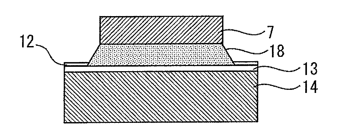
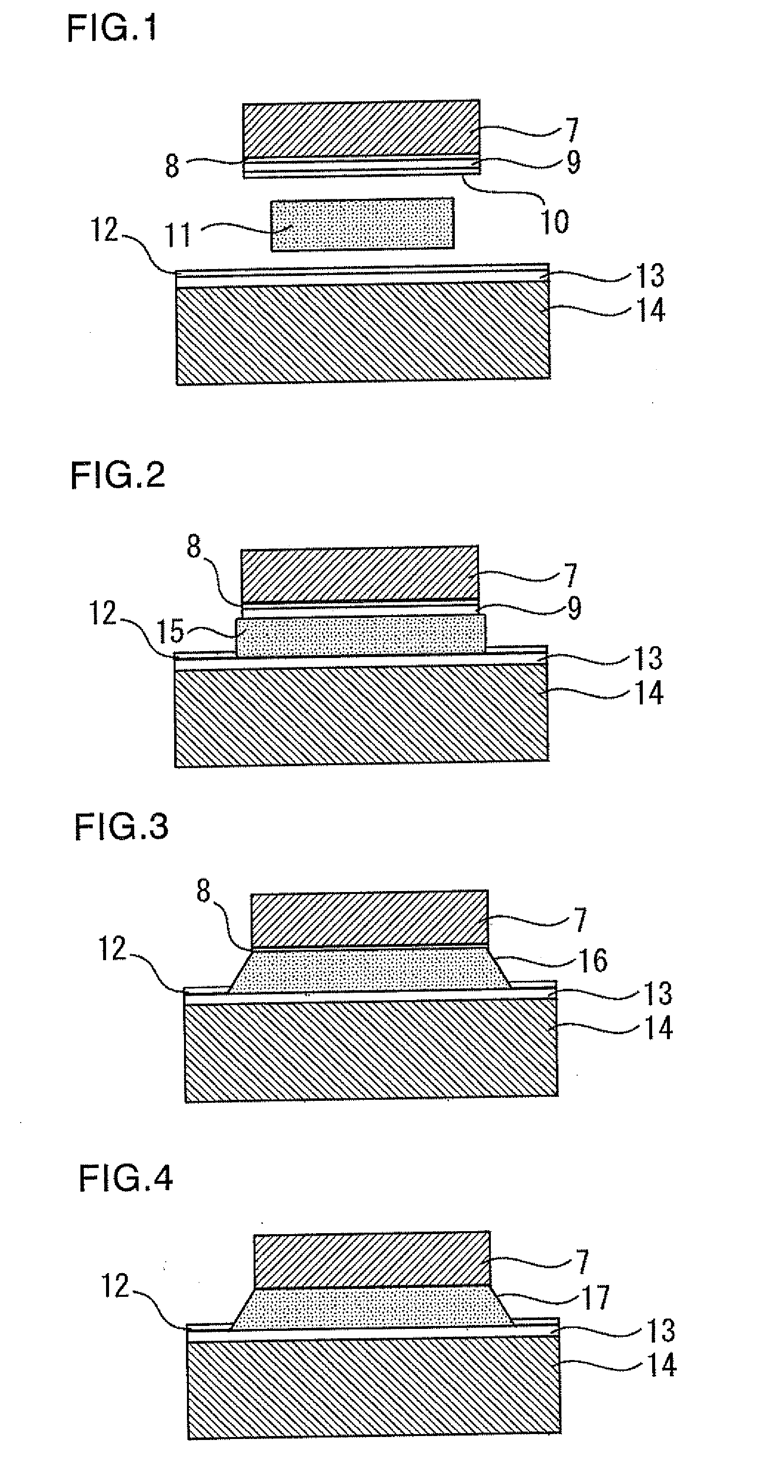
[0025]FIGS. 1 to 5 show a semiconductor device and a die bonding method therefor according to a first embodiment of the present invention.

[0026]In a die bonding process for a semiconductor chip, the chip is usually subjected to an elevated temperature higher than the melting point of the solder, causing the solder layer to assume a liquid state. As a result, the diffusion rate of the solder becomes extremely high, leading to “abnormal diffusion” of the solder and formation of voids. To prevent this from occurring, the diffusion rate of the solder must be reduced to prevent formation of voids. This requires that, when the die bonding has been completed, the melting point of the solder be increased to higher than the die bonding temperature so that the solder returns to a solid state.

[0027]To achieve this, according to the present embodiment, a solder bonding layer metal is formed on the back surface of the semiconductor chip, and a special metal for elevating the melting point of the...

second embodiment

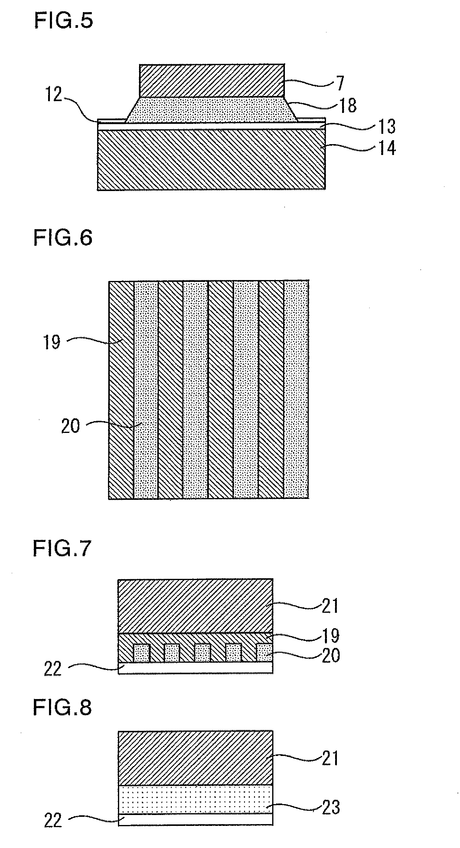
[0043]FIGS. 6 and 7 show a semiconductor device and a die bonding method therefor according to a second embodiment of the present invention. Although the first embodiment has been described with reference to the case where the melting point elevating metal 9 is Ti, the melting point elevating metal 9 may be Pt with the same effect.

[0044]According to the present embodiment, the melting point elevating metal 9 is deposited in stripes on the back surface of the semiconductor chip to allow the metal to uniformly diffuse into the solder.

[0045]FIG. 6 shows the back surface of the semiconductor chip with the oxidation inhibiting metal 22 removed, and FIG. 7 shows a cross-sectional view of the semiconductor chip.

[0046]Referring to FIGS. 6 and 7, the semiconductor chip comprises a melting point elevating metal 19, a solder bonding layer metal 20; a semiconductor substrate 21, and a metal 22 for improving solder wetting property or inhibiting oxidation. This arrangement allows the melting poi...

third embodiment

[0048]FIG. 8 shows a cross-sectional view of a semiconductor chip of a semiconductor device according to a third embodiment of the present invention. In this semiconductor device, powdered metal having a melting point elevating effect is uniformly mixed in the solder bonding layer.

[0049]Referring to FIG. 8, the semiconductor chip comprises a semiconductor substrate 21 and a solder bonding layer metal 23 uniformly containing the melting point elevating metal 19 of the second embodiment. Reference numeral 22 shows a metal for improving solder wetting property or inhibiting oxidation.

[0050]Thus, according to the present embodiment, in the solder bonding layer metal 23, the melting point elevating metal 19 is powdered and mixed in the solder bonding layer metal 20 to allow the melting point elevating metal 19 to uniformly diffuse into the solder.

[0051]Thus, the present embodiment has the same effect as the second embodiment. Furthermore, since the melting point elevating metal 19 is pow...


PUM

PropertyMeasurementUnit
temperatureaaaaaaaaaa
wetting propertiesaaaaaaaaaa
semiconductoraaaaaaaaaa

Abstract

A semiconductor device includes a semiconductor substrate, a first metal film on a back surface of the semiconductor substrate, a second metal film on the first metal film, and a third metal film on the second metal film. The first metal film forms an alloy with a solder. The second metal film causes isothermal solidification of the solder. The third metal film improves solder wetting properties or inhibits oxidation. Further, in a method for die-bonding a semiconductor device, a specific metal is diffused into a solder, when the solder melts, to transform the solder into a high melting point alloy, thereby causing isothermal solidification of the solder. The specific metal is different from the metal of the solder.

Description

FIELD OF THE INVENTION[0001]The present invention relates to a semiconductor device and a die bonding method therefore. The present invention is preferably used when a semiconductor device is kept at high temperature for a long time during soldering process.BACKGROUND ART[0002]In the case of a quad flat no-lead (QFN) package manufacturing process that molds a plurality of packages together and that requires the semiconductor chips to be die-bonded by use of a high melting point solder such as AuSn eutectic solder, the chips are usually subjected to elevated temperature for a long time using a heater.[0003]Specifically, the semiconductor chips are exposed to high temperature conditions until their die boding is complete. Therefore, during this die bonding process, the solder as the bonding material is in a liquid state and hence rapidly diffuses. If this diffusion proceeds extremely, the solder may reach the base material of the lead frames beyond the barrier metal, for example. This...

Claims


Application Information

Patent Timeline
Patent Type & Authority Applications(United States)
IPC IPC(8): H01L23/48
CPCH01L23/49513H01L24/29H01L24/83H01L2224/04026H01L2224/29144H01L2224/83101H01L2224/83801H01L2224/83825H01L2924/01029H01L2924/01033H01L2924/01042H01L2924/0105H01L2924/01078H01L2924/01079H01L2924/01082H01L2924/01094H01L2924/01322H01L2924/10329H01L2924/0132H01L2224/29H01L2224/29298H01L2924/00013H01L2924/01006H01L2924/01023H01L2924/01041H01L2924/014H01L2224/29101H01L2224/13099H01L2924/00H01L2224/29111H01L24/32H01L2924/01028H01L2924/157H01L2224/29299H01L2224/2929H01L2224/29099H01L2224/29199H01L2224/32245H01L2924/00014
Inventor ITO, MASAYASUMIYAWAKI, KATSUMIFUJINO, JUNJI
Owner MITSUBISHI ELECTRIC CORP
Why Eureka
Try Eureka