Method of producing a semiconductor device, and wafer-processing tape

Active Publication Date: 2007-06-21
FURUKAWA ELECTRIC CO LTD
View PDF9 Cites 70 Cited by
  • Summary
  • Abstract
  • Description
  • Claims
  • Application Information

AI Technical Summary

Benefits of technology

[0033] The flip-chip packaging method for a wafer having metal electrodes, by using the wafer-processing tape, according to the present invention, exhibits a significant effect in form

Problems solved by technology

The method using a lead frame, which method has been used for packaging a semiconductor device so far, fails to cope with the demand for such high-density packaging.
If a semiconductor device connected by such a flip-chip is used as it is, the electrode of the connected portion is exposed to the air, and large stress is applied to the connected portion of the bump through thermal history in the subsequent step of, for example, a solder reflow step, because of a large difference in the thermal expansion coefficient between a chip and a substrate, giving rise to a problem concerning packaging reliability.
However, it has been found that a removable adhesive or adhesion agent used for bonding after UV curing for this purpose has difficulty in retaining resin fluidity, due to the formation of a three-dimensional crosslinking structure associated with UV radiation.
Therefore, the filler cannot satisfactorily be filled into the substrate irregular surface, rendering it impossible to obtain bonding reliability.
In the meantime, generally, semiconductor elements subjected to flip-chip packaging have many electrodes, and also these electrodes are arranged around the semiconductor element because of a circuit design problem.
Therefore, if a liquid resin is poured from the gap between electrodes of these semiconductor elements by a capillary phenomenon when a resin paste is filled, the resin spreads insufficiently, which readily allows

Method used


Image

  • Method of producing a semiconductor device, and wafer-processing tape
  • Method of producing a semiconductor device, and wafer-processing tape
  • Method of producing a semiconductor device, and wafer-processing tape

Examples


examples

[0066] Each of the characteristics in the following examples were tested and evaluated, according to the following tests. The “part(s)” means a part(s) by mass. [0067] 1. Gel fraction: About 0.05 g of the removable adhesive layer was weighed, it was dipped in 50 ml of xylene for 24 hours at 120° C., and then the resultant xylene was filtered through a stainless-steel net of 200 meshes, and the resultant insoluble constituents remained on the net were dried for 120 minutes at 110° C. Then, the mass of the thus-dried insoluble constituents was weighed, to determine a gel fraction, according to the formula shown below: Gel fraction (%)={(Mass of insoluble constituents) / (mass of weighed removable adhesive layer)}×100 [0068] 2. Removable adhesive double bond amount: The amount of carbon-carbon double bond contained in about 10 g of the heated and dried removable adhesive agent was measured and quantitatively determined by a mass increasing method by bromine addition reaction in a dark pl...

examples 1 to 7

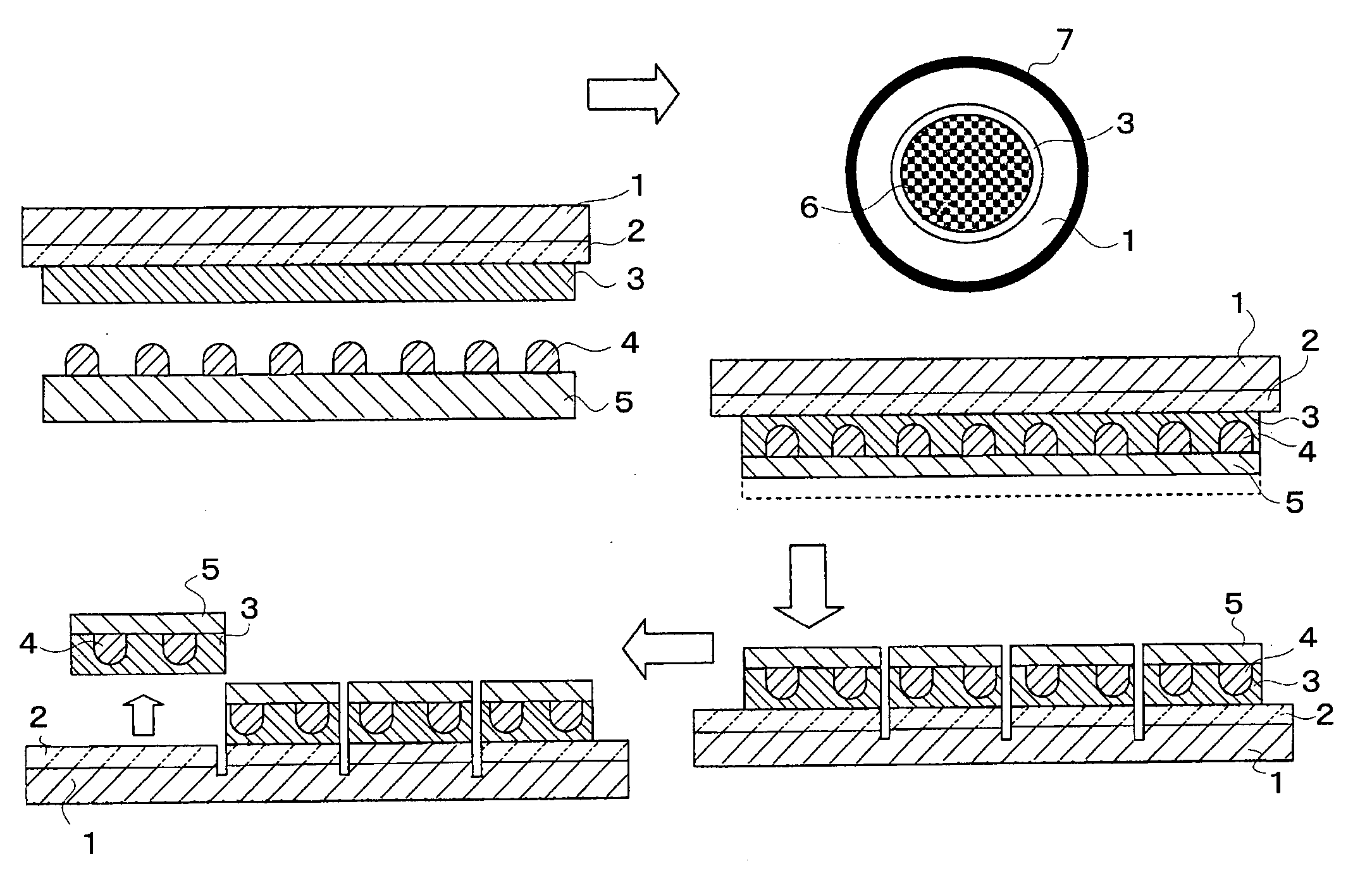
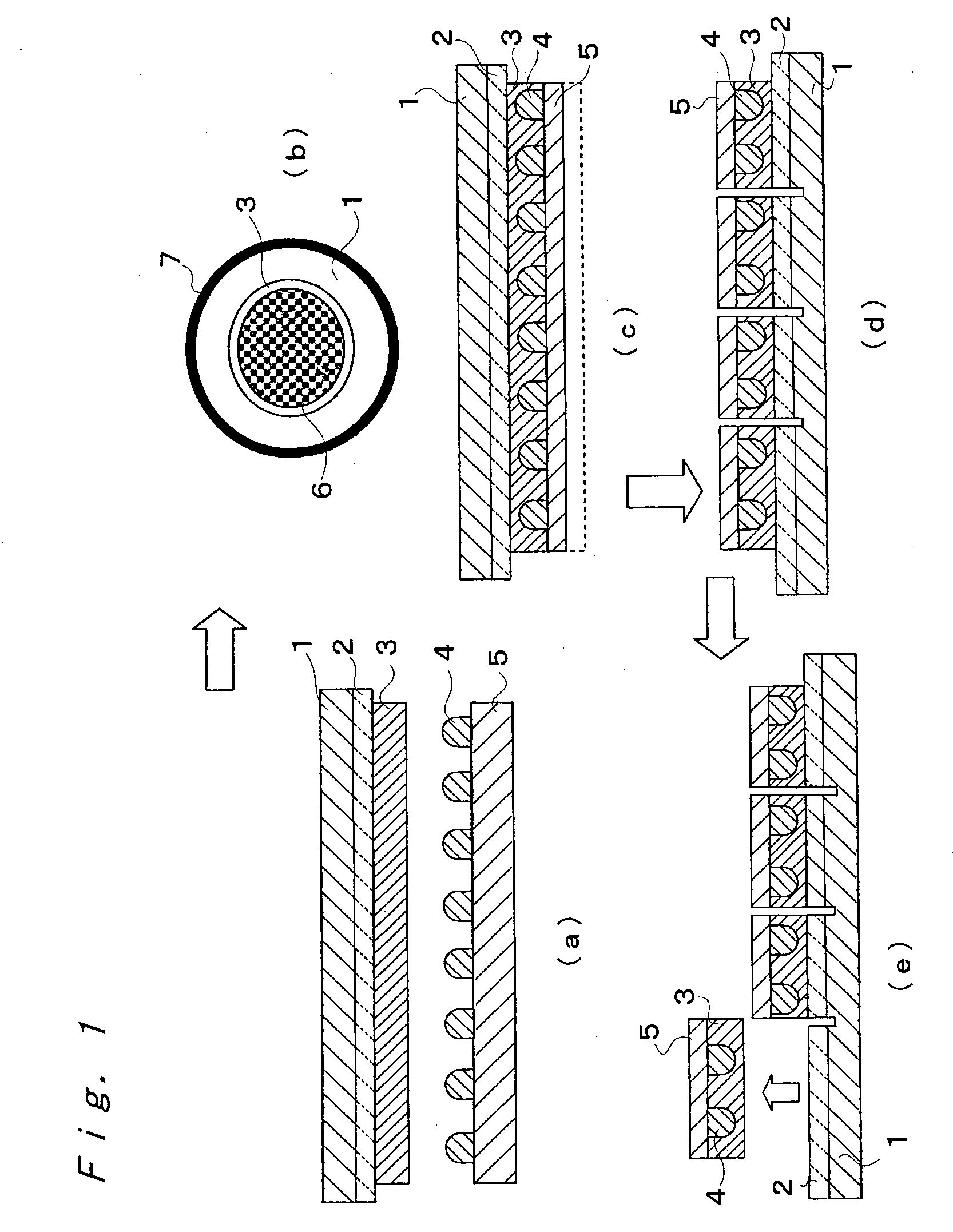
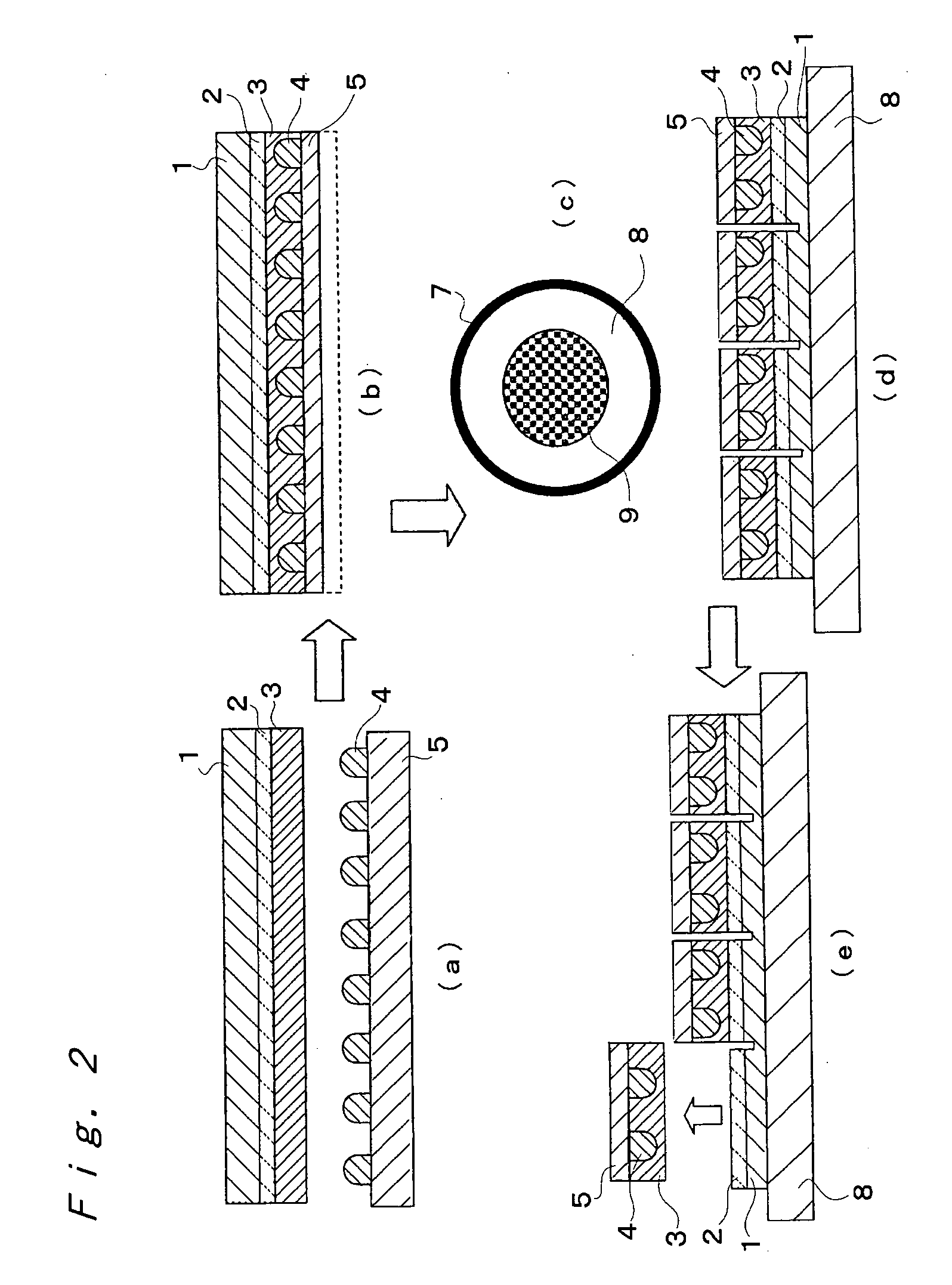
[0089] Any one of the wafer-processing tapes obtained by the combinations, as shown in Table 1, from which the carrier film had been peeled off, was, respectively, adhered to a 5-inch wafer with a gold stud bump under heating on a hot plate at 80° C., and then the backside of the circuit substrate was ground using a backside grinder, to make the circuit substrate have a finish thickness of 50 μm. Then, the circuit substrate was irradiated with UV at a dose of 1,000 mJ / cm2 in the state that the processing tape was adhered to the circuit substrate, followed by dicing into chips each of which was 10 mm×10 mm square. The resultant chips were picked up by a pickup die bonder, and flip chips were packaged in accordance with the electrode position of the resin substrate, to produce a semiconductor device.

TABLE 1Example 1Example 2Example 3Example 4Example 5Example 6Example 7Support of protective tapePEPEPEPEPEPEPEProtective tape removable adhesive agent1A2A3A4A5A6A—compositionCompound (A)...


PUM

PropertyMeasurementUnit
Temperatureaaaaaaaaaa
Fractionaaaaaaaaaa

Abstract

A wafer-processing tape, having a removable adhesive layer(2), and an adhesive layer (3), formed on a substrate film(1), wherein the tape is used in a process involving the steps of: grinding a back face of a wafer circuit substrate (5) having convex-type metal electrodes (4), and dicing the wafer circuit substrate into chips, in a state that the tape is adhered to the wafer circuit substrate; and picking up the chips, in which the chips are picked up in a state that the adhesive layer (3) is peeled from the substrate film (1) but is bonded to the individual chip.

Description

TECHNICAL FIELD [0001] The present invention relates to a method of producing a semiconductor device, and it also relates to a wafer-processing tape that can be used in the same. BACKGROUND ART [0002] Along with the recent development of small-sized and thinner-type electronic machinery and tools (electronic devices), there has been strong demand for the establishment of higher-density packaging technique of semiconductor elements. The method using a lead frame, which method has been used for packaging a semiconductor device so far, fails to cope with the demand for such high-density packaging. Also, a method of primarily using a resin paste, among die bonding materials used for bonding these, is currently dominant. [0003] For this, flip-chip packaging is proposed as a method to package a semiconductor device having the substantially same size as a semiconductor element. This flip-chip packaging has attracted remarkable attention as a method of packaging semiconductor elements in a ...

Claims


Application Information

Patent Timeline
IPC IPC(8): B32B37/12B32B38/10B32B38/04B32B7/12B32B15/04C09J7/20
CPCH01L21/67092Y10T428/2848H01L21/6835H01L21/6836H01L21/78H01L24/27H01L24/83H01L24/90H01L2221/68327H01L2221/6834H01L2224/1134H01L2224/16H01L2224/274H01L2224/73203H01L2224/83191H01L2224/83851H01L2224/90H01L2924/01005H01L2924/01013H01L2924/01015H01L2924/01027H01L2924/01033H01L2924/01074H01L2924/01078H01L2924/01079H01L2924/01082C09J7/02C09J2201/36C09J2203/326C09J2433/00C09J2463/00C09J2479/08H01L21/561H01L21/563H01L24/29H01L2924/00013H01L2924/01006H01L2924/01019H01L2924/014H01L21/67132Y10T156/1052Y10T428/2852Y10T428/28Y10T156/1062H01L2224/81191H01L2224/293H01L2224/2929H01L2221/68377H01L2224/73104H01L2224/13099H01L2924/3512H01L2924/00H01L2924/00014H01L2924/0665C09J7/20C09J2301/208H01L2224/27436
Inventor MORISHIMA, YASUMASAKITA, KENJIISHIWATA, SHINICHIYAMAKAWA, TAKANORI
Owner FURUKAWA ELECTRIC CO LTD
Why Eureka
Try Eureka