Transconductor, integrator, and filter circuit

a filter circuit and integrator technology, applied in the field of transconductor, can solve the problems of increasing chip area and power consumption, low-power complex filter, and increasing common-mode potential, so as to reduce power consumption and chip area, and improve noise characteristics

Active Publication Date: 2007-06-28
PANASONIC SEMICON SOLUTIONS CO LTD
View PDF9 Cites 24 Cited by
  • Summary
  • Abstract
  • Description
  • Claims
  • Application Information

AI Technical Summary

Benefits of technology

[0012] In view of the above-described problems, an object of the present invention is to provide a fully differential transconductor in which a common-mode operating point of a differential output is stabilized, power consumption and a chip area are reduced, and noise characteristics are improved. Another object of the present invention is to provide an integrator and a filter circuit comprising the transconductor.
[0014] Thereby, the single-end outputs of the first and second transconductors whose inversion input terminal and non-inversion input terminal are connected to each other are differential outputs of the transconductor of the present invention. Therefore, the common-mode operating point is robust with respect to a common-mode change in the differential input. Therefore, the common-mode operating point of the differential output can be stabilized without particularly providing a common-mode feedback circuit, so that the power consumption and the chip area can be reduced. Also, a noise generating factor, such as a current source for stabilizing a common-mode voltage or the like, does not need to be connected to a signal line, thereby making it possible to improve the noise characteristics.
[0017] Thereby, since the first and second voltage-to-current conversion circuits are implemented using, for example, a differential pair of transistors whose sources are grounded, thereby making it possible to further reduce the power consumption and improve the linearity.
[0019] Thereby, a common-mode operating voltage of the differential output can be stabilized and kept accurately at a desired voltage. Note that, since the transconductor has a small common-mode gain, a gain of the common-mode feedback loop can be reduced, so that an increase in power consumption and chip area and a deterioration in noise characteristics due to addition of the common-mode feedback circuit do not cause a problem.
[0030] Thereby, the capacitor connected between the output terminal of each of the first and second transconductors and the output terminal of the common-mode feedback circuit functions not only as a filter capacitor but also as a phase compensating capacitor of common-mode feedback, resulting in a stabler common-mode operating point of the differential output.
[0032] Thereby, each of the capacitors connected between the input and output terminals of the current mirror circuits plays a role not only in serving as a filter capacitor but also in canceling a signal delay in the current mirror circuit, resulting in an improvement in radio-frequency characteristics of the integrator.

Problems solved by technology

Therefore, it is also one of important challenges to achieve a low-power complex filter.
Particularly, when a complex filter is composed of a fully differential Gm-C filter, a common-mode potential becomes considerably unstable due to the structure of the complex filter, and therefore, a lager-scale common-mode feedback circuit is required.
However, the large common-mode feedback circuit is responsible for an increase in chip area and power consumption.
Also, a common-mode current in a signal line may be increased so as to stabilize the common-mode potential, however, this leads to a deterioration in noise characteristics.
However, such a common-mode feedback circuit has large power consumption, and prevents the reduction of the power of a chip.
Also, a noise generating factor, such as a current source or the like, is connected to a signal line, leading to a deterioration in noise characteristics.
Also, a relatively large phase compensating capacitor is required to stabilize the common-mode feedback, leading to an increase in chip area.

Method used


Image

  • Transconductor, integrator, and filter circuit
  • Transconductor, integrator, and filter circuit
  • Transconductor, integrator, and filter circuit

Examples


first embodiment

[0046] (First Embodiment)

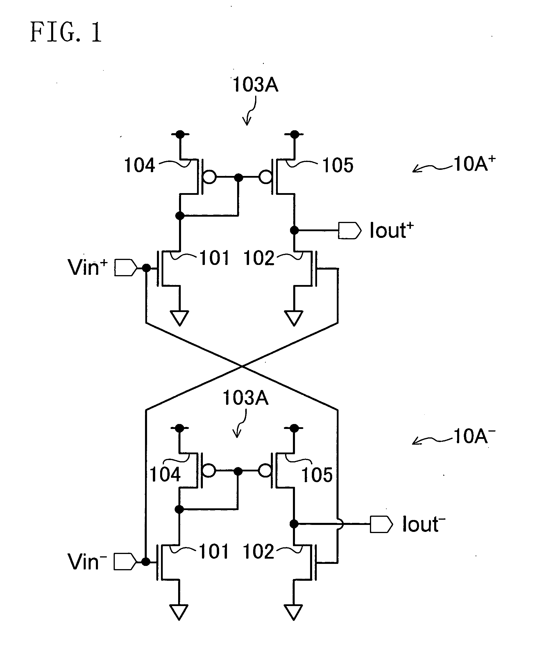
[0047]FIG. 1 illustrates a configuration of a transconductor according to a first embodiment. This transconductor comprises transconductors 10A+ and 10A− each of which receives a differential voltage signal and outputs a single-end current signal. An inversion input terminal of one of the transconductors 10A+ and 10A− is connected with a non-inversion input terminal of the other. Differential voltage signals (Vin+-Vin−) and (Vin−-Vin+) are input to the input transconductors 10A+ and 10A−, respectively. Current signals Iout+ and Iout− are output from single-end output terminals of the transconductors 10A+ and 10A−, respectively.

[0048] Specifically, the transconductor 10A (a superscript is removed when the transconductors 10A+ and 10A− are not distinguished from each other, and the same applies to the other reference characters) comprises transistors 101 and 102 (voltage-to-current conversion circuits) and a current mirror circuit 103A. The current mirror cir...

second embodiment

[0055] (Second Embodiment)

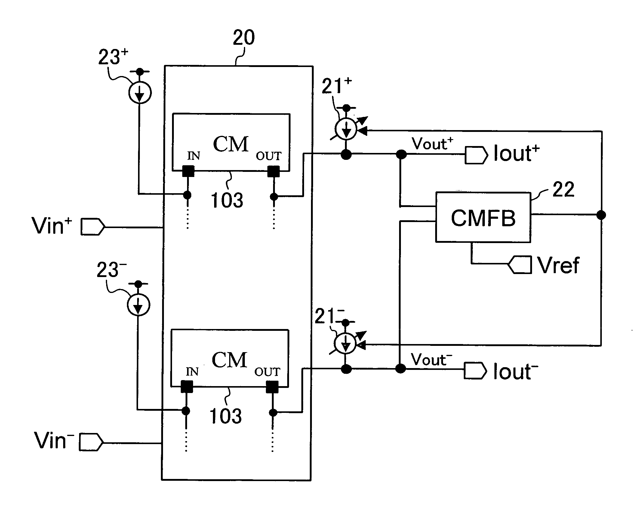
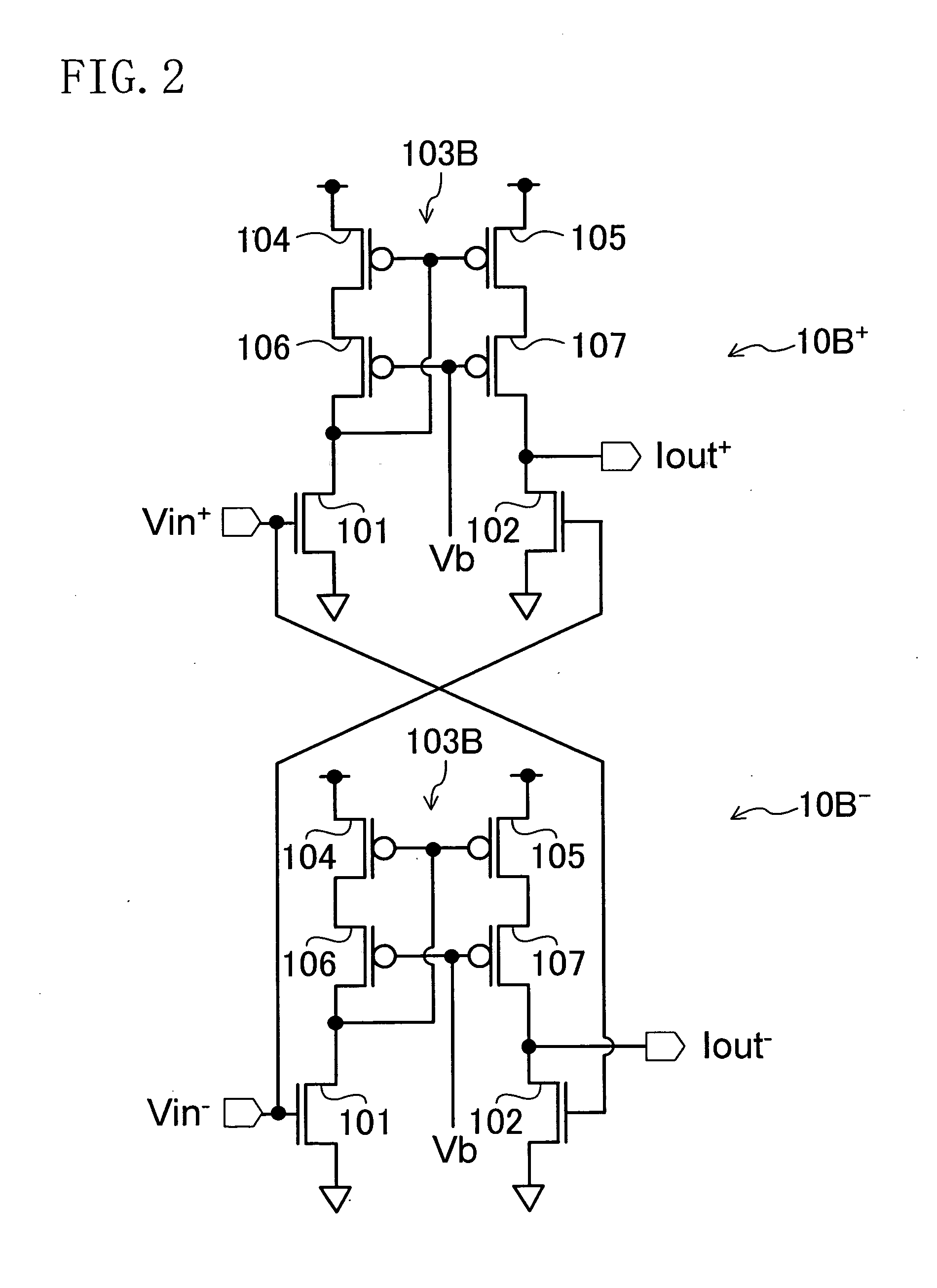
[0056] In the transconductor of the first embodiment, for example, as illustrated in FIG. 1, the transistors 101 and 102 having the pseudo-differential configuration are used to perform voltage-to-current conversion. Therefore, the gm value of the transconductor is equal to the gm value of each of the transistors 101 and 102. In other words, the gm value of the transconductor of the first embodiment is influenced by the common-mode operating point of the differential voltage signal (Vin+-Vin−). More specifically, an operating point of the differential output of the transconductor of the first embodiment varies depending on ambient temperature, a power supply voltage, a process variation, and the like as well as an input operating point. A change in the output operating point particularly causes a deterioration in characteristics of applications in which a plurality of transconductors are connected in cascade, such as, for example, a Gm-C filter as illustrat...

third embodiment

[0067] (Third Embodiment)

[0068] An integrator is constructed by adding a capacitor to the transconductor of each embodiment above. For example, in the case of the transconductor of FIG. 4, there are three portions to which a capacitor is connected: between the differential output terminals; between the differential output terminal and the output terminal of the common-mode feedback circuit 22; and between the input and output terminals of the current mirror circuit 103. FIG. 6 illustrates a configuration of an integrator according to a third embodiment. This integrator is obtained by adding capacitors 31, 32+ and 32−, and 33+ and 33− to the above-described three portions of the transconductor of FIG. 4. The capacitor 31 is connected between the differential output terminals of the transconductor. The capacitors 32+ and 32− are each connected between the differential output terminal and the output terminal of the common-mode feedback circuit 22. The capacitors 33+ and 33− are each co...


PUM


Abstract

A transconductor for receiving a differential voltage signal and outputting a differential current signal, includes two transconductors for receiving the differential voltage signal and outputting a single-end current signal. An inversion input terminal of one of the two transconductors is connected with a non-inversion input terminal of the other. The transconductor outputs a current signal output from each of the two transconductors as the differential current signal.

Description

CROSS REFERENCE TO RELATED APPLICATIONS [0001] This Non-provisional application claims priority under 35 U.S.C. §119(a) on Patent Application No. 2005-378685 filed in Japan on Dec. 28, 2005, the entire contents of which are hereby incorporated by reference. BACKGROUND OF THE INVENTION [0002] 1. Field of the Invention [0003] The present invention relates to a transconductor, and more particularly, to a fully differential transconductor whose input and output are all differential signals, and an integrator and a filter circuit comprising the transconductor. [0004] 2. Description of the Related Art [0005] Complex filters for use in Low-IF radio architecture play a role in efficiently eliminating an aliasing image signal in the same band in which desired waves are present, in the course of down conversion. By using the complex filter, an image eliminating filter having a high Q value is no longer required. Therefore, the complex filter is recognized as an important part for development ...

Claims


Application Information

Patent Timeline
Patent Type & Authority Applications(United States)
IPC IPC(8): G06G7/12
CPCH03F3/45475H03H11/0433H03H2011/0494
Inventor MORIE, TAKASHIMATSUMOTO, AKINORIDOSHO, SHIRO
Owner PANASONIC SEMICON SOLUTIONS CO LTD
Why Eureka
Try Eureka