Measuring method for optical transfer function, image restoring method, and digital imaging device

a technology of optical transfer and image restoration, applied in the field of measuring methods for optical transfer function, image restoration method, digital imaging device, can solve the problems of difficult image degradation, and inability to improve the resolution performance of imaging optical system, so as to achieve the effect of easy calculation, optical, and no increase in the processing load of digital imaging devi

Inactive Publication Date: 2007-06-28
PANASONIC CORP
View PDF0 Cites 35 Cited by
  • Summary
  • Abstract
  • Description
  • Claims
  • Application Information

AI Technical Summary

Benefits of technology

[0009] According to this configuration, the imaging optical system and the image sensor actually arranged in an imaging camera is used to calculate an optical transfer functions. Accordingly, it is possible to calculate an optical transfer functions reflecting the image degradation factor occurring in the imaging optical system and the image degradation factor ascribable to inter-element crosstalk. Also, the elements constituting the imaging area of an imaging camera are scanned by light incident through the imaging optical system arranged in the imaging camera, and optical transfer functions are calculated based on an image obtained by performing the scanning. Accordingly, optical transfer functions can easily be calculated without dismantling the imaging camera.
[0051] According to the present invention, an image created with a digital imaging device is associated with the degradation factor information for correcting the image degraded due to the imaging means of the digital imaging device, and then outputted, and a correction is performed in an image correction server apparatus of the output destination. Accordingly, the present invention has an advantageous effect in that a corrected image can be obtained by performing a deconvolution processing without increasing the processing load of the digital imaging device.

Problems solved by technology

In such miniaturized and thickness-reduced imaging cameras, the image is degraded due to lens aberration and the like, and thus it is difficult to improve the resolution performance of imaging optical systems.
In conventional miniaturized and thickness-reduced imaging cameras, the resolution of image sensors has been raised, but the resolution performance of imaging optical systems has not been improved.
Consequently, high-quality images corresponding to the improvement of image sensor resolution cannot be achieved.
Consequently, it may be impossible to restore the image with fidelity by performing a deconvolution processing using the optical transfer function calculated by the above described method.
Accordingly, the optical transfer function measurement is not easy to perform.
As the number of pixels of the digital imaging device becomes large, the processing load of deconvolution processing increases.
When the processing load increases, the digital imaging device requires a high-speed CPU and a high-capacity memory, and at the same time consumes more power.
When the digital imaging device is a portable apparatus driven by a battery, the increase of power consumption poses a problem.

Method used


Image

  • Measuring method for optical transfer function, image restoring method, and digital imaging device
  • Measuring method for optical transfer function, image restoring method, and digital imaging device
  • Measuring method for optical transfer function, image restoring method, and digital imaging device

Examples


first embodiment

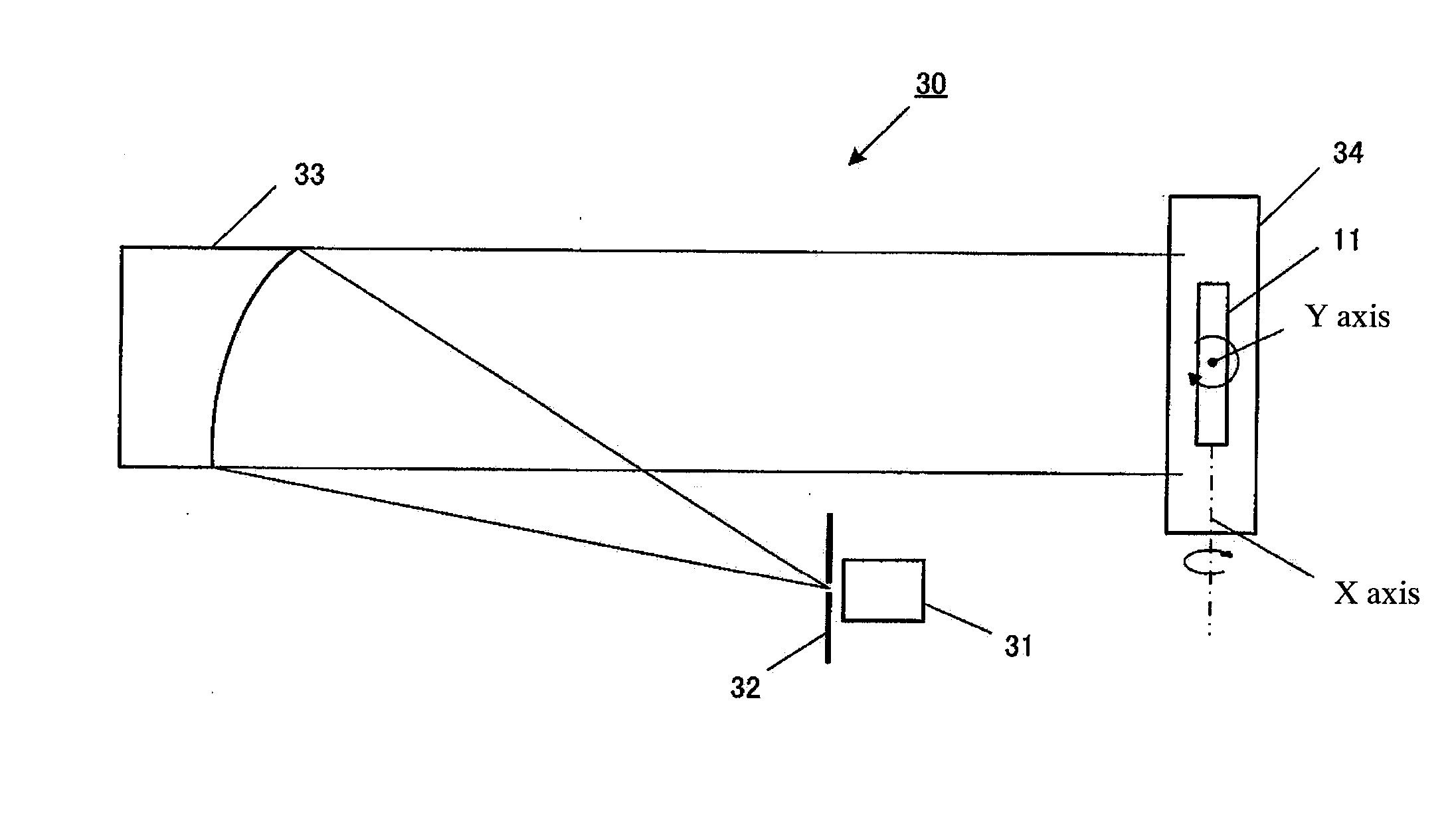
[0072]FIG. 1 is a view showing a spread function measurement apparatus according to a first embodiment of the present invention. Referring to FIG. 1, the spread function measurement apparatus 30 includes a light source 31, a pinhole board 32, an off-axis paraboloid mirror 33 and a camera holding mechanism 34. The spread function measurement apparatus 30 is an apparatus for measuring spread functions of an imaging camera provided with an imaging optical system and an image sensor such as a CCD or CMOS sensor. The light source 31 emits light having wavelength characteristics containing specification characteristics of an imaging camera to be measured. The pinhole board 32 is arranged in the vicinity of the light source 31. After passing through a pinhole of the pinhole board 32, the irradiating-light as divergent ray is incident on the off-axis paraboloid mirror 33. Reflected on the off-axis paraboloid mirror 33, the irradiating-light becomes collimated light with no color aberration....

second embodiment

[0099] A second embodiment of the present invention will now be described.

[0100] According to the first embodiment described above, the rotation of the imaging camera 11 allows irradiating-light to move relatively on the imaging area of image sensor, whereby elements to be measured are scanned. According to the present embodiment, the imaging camera 11 remains fixed, and the position of irradiating-light is changed, whereby elements to be measured are scanned.

[0101]FIG. 6 is a configuration diagram of a spread function measurement apparatus according to the present embodiment. As shown in FIG. 6, in the spread function measurement apparatus 40, light irradiated from a light source 41 passes through a pinhole of a pinhole board 42 and is reflected on an off-axis paraboloid mirror 43 and becomes collimated light. Then the collimated irradiating-light is reflected on a reflecting mirror 45 and incident on the imaging optical system of an imaging camera 11 held in a camera holding mec...

third embodiment

[0104] A third embodiment of the present invention will now be described.

[0105] In the spread function measurement apparatus 30 according to the first embodiment described above, the pinhole board 32 is arranged in the vicinity of the light source 31, whereby a point-like irradiating-light image is projected on the imaging area. According to the present embodiment, instead of the pinhole board 32, a slit board is provided, whereby the image sensor is scanned with linear irradiating-light.

[0106]FIG. 7 is a configuration diagram of a spread function measurement apparatus according to the present embodiment. As shown in FIG. 7, in the spread function measurement apparatus 50, a slit board 52 is arranged in the vicinity of a light source 51. The slit board 52 is held in a slit holding mechanism 56. The slit holding mechanism 56 has a mechanism that rotates the slit board 52 so that the longitudinal direction of the slit is adjusted to a longitudinal direction or a lateral direction. I...


PUM


Abstract

In an measuring method for optical transfer function of the invention, irradiating-light from a light source (31) scans an element to be measured within an image sensor of an imaging camera constituted by integrating an imaging optical system and the image sensor. The element to be measured converts sequentially the irradiating-light into an electrical signal and outputs the electrical signal. Further, based on the outputted electrical signal, point spread function data is generated, and subjected to Fourier transform to calculate an optical transfer function. Accordingly, a method is provided for measuring an optical transfer function for properly restoring image degradation due to factors including the position of the imaging optical system within the imaging camera and inter-element cross talk.

Description

TECHNICAL FIELD [0001] The present invention relates to a measuring method for optical transfer function used to correct an image created with an imaging camera to obtain an image close to the original image, and an image restoring method. BACKGROUND ART [0002] In recent years, the configuration of imaging cameras has been miniaturized and thickness-reduced. Accordingly, the overall length of imaging optical systems has been shortened, and the number of constituent lenses has also been reduced. In such miniaturized and thickness-reduced imaging cameras, the image is degraded due to lens aberration and the like, and thus it is difficult to improve the resolution performance of imaging optical systems. In conventional miniaturized and thickness-reduced imaging cameras, the resolution of image sensors has been raised, but the resolution performance of imaging optical systems has not been improved. Consequently, high-quality images corresponding to the improvement of image sensor resolu...

Claims


Application Information

Patent Timeline
Patent Type & Authority Applications(United States)
IPC IPC(8): G01M11/00G06T3/00G06T5/00H04N5/225
CPCG06T5/003G06T5/006G06T5/10G06T2207/20056
Inventor ARAKI, NOBUHIROWARAGAI, KATSUNORI
Owner PANASONIC CORP
Why Eureka
Try Eureka