

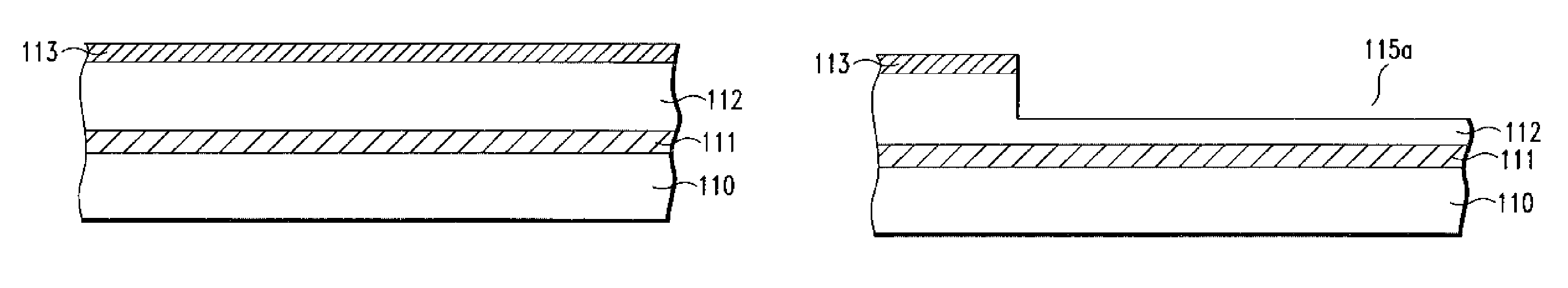
OPTIMIZED SiCN CAPPING LAYER
a silicon nitride and capping layer technology, applied in the direction of semiconductor devices, semiconductor/solid-state device details, electrical apparatus, etc., can solve the problems of h still not having the desired oxygen barrier properties possessed by silicon nitride, adversely affecting the reliability of ic chips, and relative high electromigration rate, etc., to achieve the effect of improving the structure of semiconductor interconnects
- Summary
- Abstract
- Description
- Claims
- Application Information
AI Technical Summary
Benefits of technology
Problems solved by technology
Method used
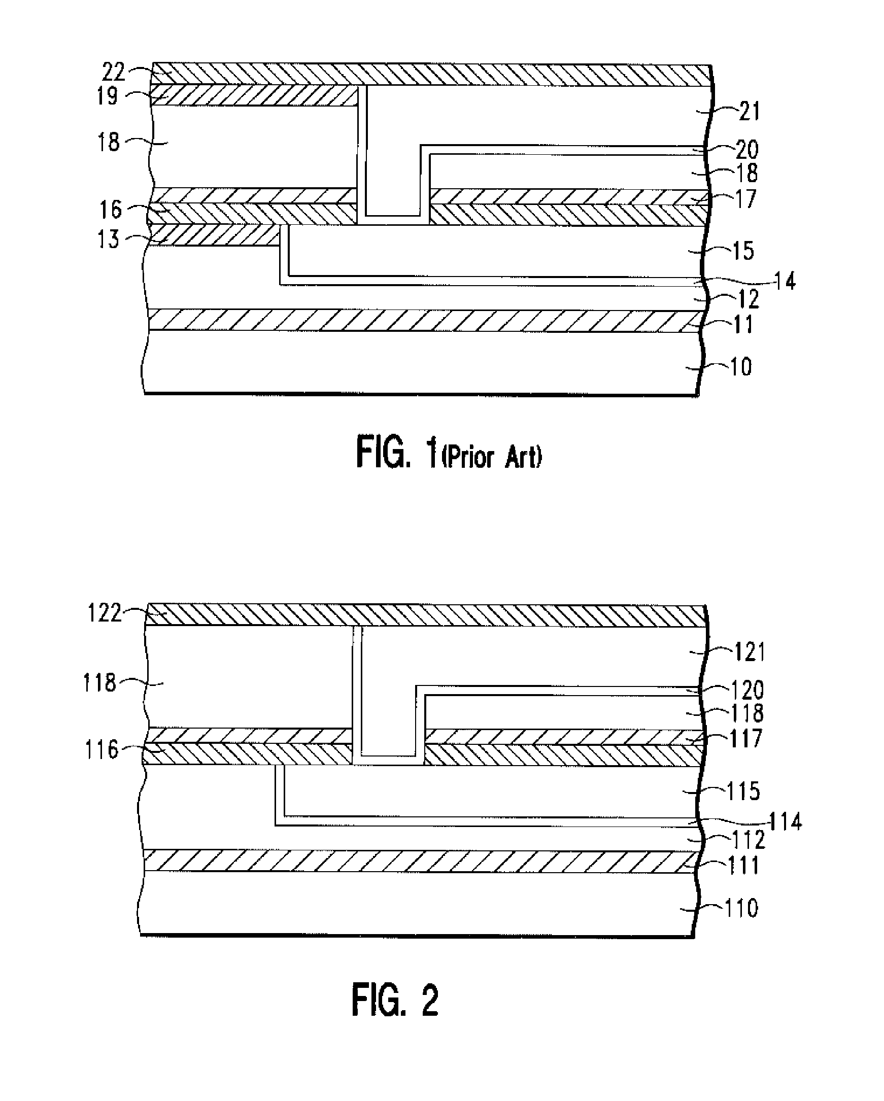
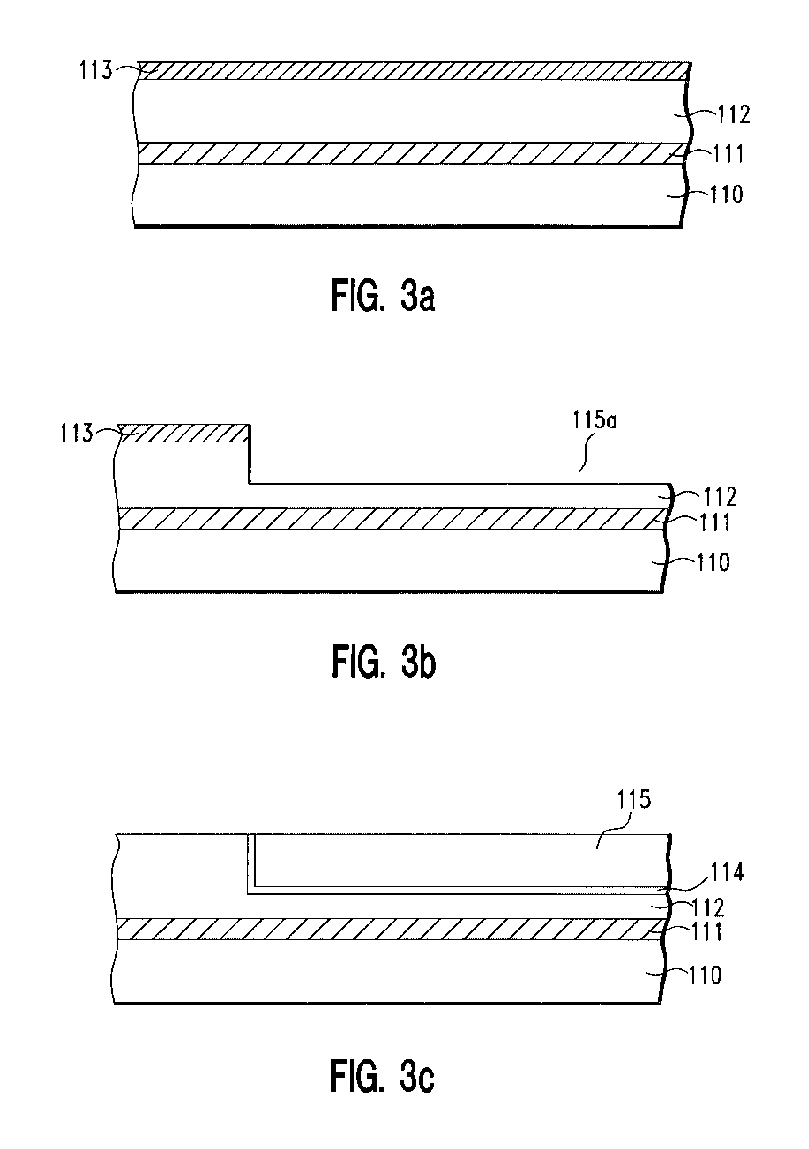
Image

Examples
example 1
[0055] When utilizing a 300 mm PECVD reactor, the optimized process ranges have been listed previously and are summarized here.
Processing condition300mm PECVD reactorTemperature300-400°C.RF Power400-800W3 MS or 4 MS flow rate50-500sccmHe flow rate50-2000sccmN2 or NH3 flow rate800-2000sccm
[0056] For deposition temperature of 400° C., the specific conditions are 3MS flow of 450 sccm, NH3 flow of 1740 sccm, He flow of 730 sccm, and RF plasma power of 480 watts. The higher deposition temperature leads to a film with higher density, 2.10 g / cm3 by X-ray reflectance (XRR) as compared to 1.97 g / cm3 for the 200 mm PECVD reactor film described in U.S. Patent Application Publication 20030134495, and with a higher dielectric constant of 5.5. Although this is a compromise of dielectric constant, the higher film density leads to better barrier properties to both oxygen and copper species. Another benefit of an increased density in capping layer is that it is a good etch stop for via first proce...
example 2
[0059] The specific 300 mm PECVD conditions for the optimized 350° C. process are 3MS flow of 300 sccm, NH3 flow of 1200 sccm, He flow of 1200 sccm, and RF plasma power of 640 watts. Films deposited under these processing conditions have similar film density to the 400° C. films described in Example 1, namely 2.15 g / cm3 by XRR. The dielectric constant of these films are slightly lower than the 400° C. films, namely 5.4, indicating that density is one of the determining factors in the dielectric constant value. Therefore, diffusion barrier effectiveness is proportional to both film density and dielectric constant.
[0060]FIG. 6 shows the oxygen barrier property of this 350° C. film, by air annealing and AES depth profiling. Comparing FIG. 6 with FIG. 5 shows that the improved 350° C. processing conditions replicate both density and barrier effectiveness of the 400° C. film. By reducing the deposition temperature, the amount of hillocks occurring during deposition is reduced. This can ...
PUM
 Abstract
Description
Claims
Application Information