Methods and semiconductor structures for latch-up suppression using a buried damage layer

a technology of damage layer and semiconductor structure, which is applied in the direction of semiconductor devices, basic electric elements, electrical equipment, etc., can solve the problems of bulk cmos devices that fail, circuits cannot be easily replaced, and significant issues of bulk cmos technologies, so as to improve latch-up immunity or suppression, suppress the latch-up of bulk cmos devices, and retain cost effectiveness

Inactive Publication Date: 2007-07-12
GLOBALFOUNDRIES INC
View PDF84 Cites 66 Cited by
  • Summary
  • Abstract
  • Description
  • Claims
  • Application Information

AI Technical Summary

Benefits of technology

[0011] The present invention is generally directed to semiconductor structures and methods that improve latch-up immunity or suppression in standard bulk CMOS device designs, while retaining cost effectiveness for integration into the process flow forming the P-channel and N-channel field effect transistors characteristic of bulk CMOS devices. In accordance with an embodiment of the present invention, a semiconductor structure comprises a first doped well formed in a substrate and a second doped well formed in the substrate proximate to the first doped well. A damage layer extends within the substrate to intersect the first and second doped wells. The damage layer operates to suppress latch-up of bulk CMOS devices built using the semiconductor structure.

Problems solved by technology

Latch-up, which is precipitated by unwanted transistor action of parasitic bipolar transistors inherently present in bulk CMOS devices, may be a significant issue for bulk CMOS technologies.
The unwanted parasitic transistor action, which has various triggers, may cause the bulk CMOS device to fail.
Because the integrated circuit cannot be easily replaced in space-based platforms, the chip failure may prove catastrophic.
However, epitaxial substrates are expensive to produce and may increase the design complexity of several critical circuits, such as electrostatic discharge (ESD) protective devices.
Guard ring diffusions are costly because they occupy a significant amount of active area silicon real estate.
However, CMOS devices are expensive to fabricate using an SOI substrate, as compared to fabrication using bulk substrates.
Furthermore, SOI substrates suffer from various other radiation-induced failure mechanisms aside from latch-up.
Another disadvantage is that SOI devices do not generally come with a suite of ASIC books that would enable simple assembly of low-cost designs.
Conventional CMOS devices are susceptible to latch-up generally because of the close proximity of N-channel and P-channel devices.
This results in negative differential resistance behavior and, eventually, latch-up of the bulk CMOS device.
The low-impedance state may precipitate catastrophic failure of that portion of the integrated circuit.
Unfortunately, irreversible damage to the integrated circuit may occur almost instantaneously with the onset of the disturbance so that any reaction to exit the latched state is belated.

Method used


Image

  • Methods and semiconductor structures for latch-up suppression using a buried damage layer
  • Methods and semiconductor structures for latch-up suppression using a buried damage layer
  • Methods and semiconductor structures for latch-up suppression using a buried damage layer

Examples


Embodiment Construction

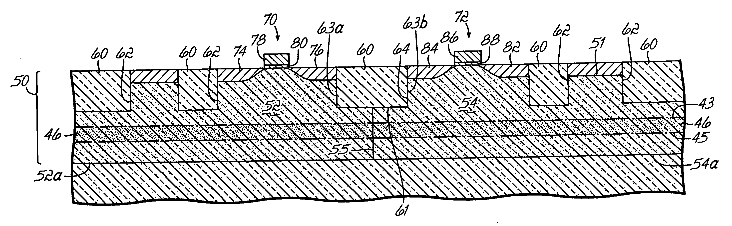
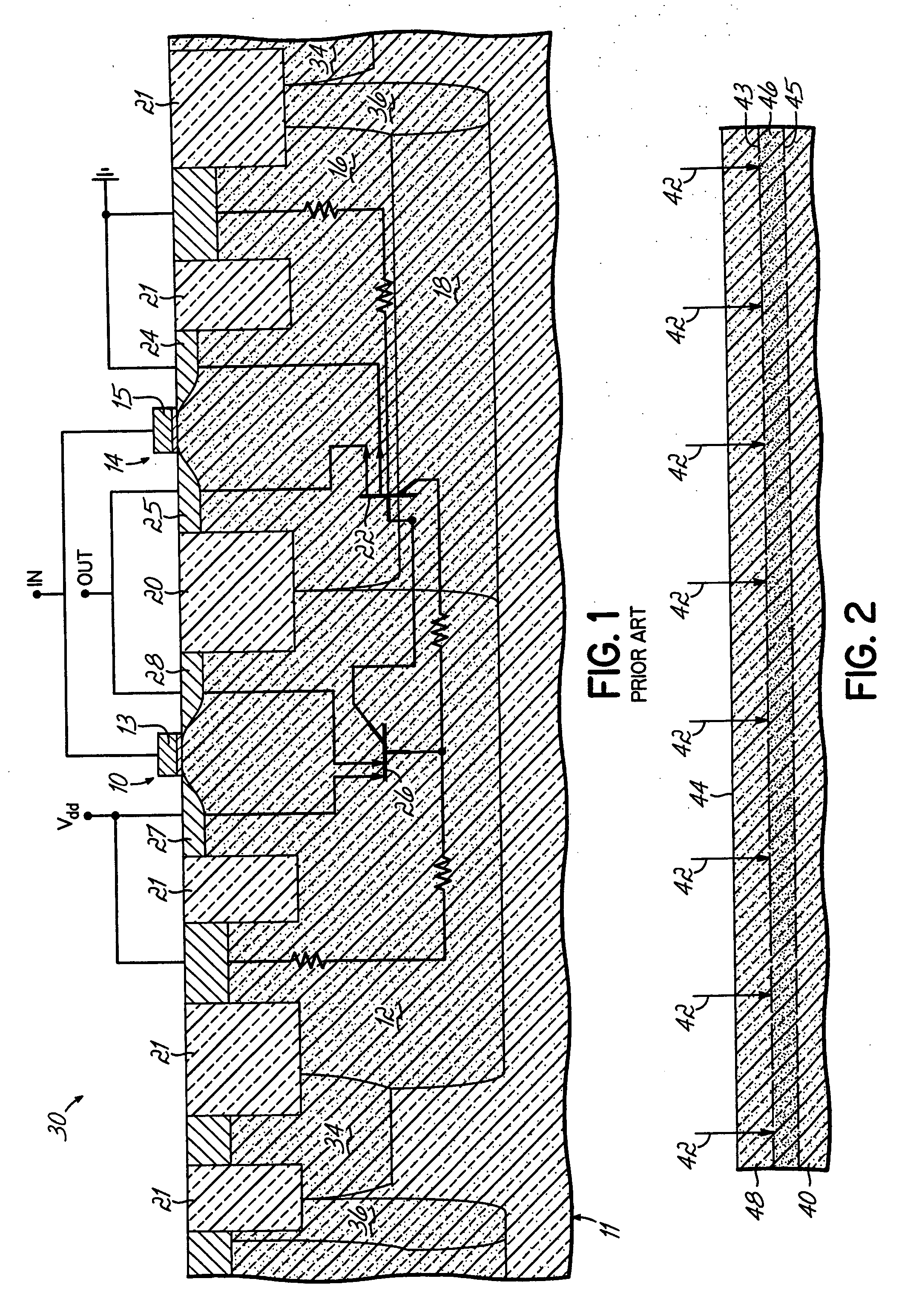
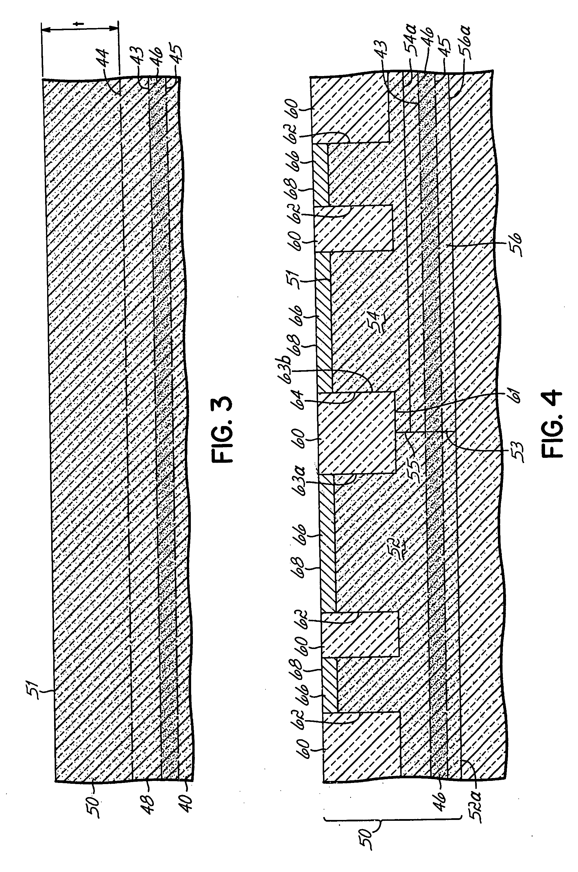
[0017] The present invention provides a buried damage layer of controlled crystalline defects formed in the base regions (N-well and P-well) of dual-well and triple-well bulk CMOS devices. The buried damage layer limits the effect of the vertical parasitic NPN structure and the lateral parasitic PNP structure responsible for latch-up in such bulk CMOS devices. The invention is advantageously implemented in the context of bulk CMOS devices where pairs of N-channel and P-channel field effect transistors are formed adjacent to each other in a P-well and an N-well, respectively, and the P-well is isolated from the N-well by a shallow trench isolation (STI) region. In a triple-well structure, the damage region may be formed through the N-well and N-band with minimal encroachment upon the junction between the N-well and P-well, which is believed to degrade the gain of the lateral parasitic PNP structure 26 (FIG. 1) while maintaining low-leakage characteristics. The buried damage layer of ...


PUM


Abstract

Semiconductor structures and methods for suppressing latch-up in bulk CMOS devices. The structure comprises a damage layer formed in a substrate, a first doped well formed in the substrate, and a second doped well formed in the substrate proximate to the first doped well. The damage layer extends within the substrate to intersect the first and second doped wells. The damage layer may be formed by ion implantation followed by growth of an epitaxial layer to segregate the active device regions from the damage layer.

Description

FIELD OF THE INVENTION [0001] The invention relates generally to semiconductor structures and methods and, in particular, to methods for suppressing latch-up in bulk complementary metal-oxide-semiconductor device structures and semiconductor structures produced by these methods. BACKGROUND OF THE INVENTION [0002] Complementary metal-oxide-semiconductor (CMOS) technologies integrate P- and N-channel field effect transistors (FETs) to form an integrated circuit using a semiconductor substrate. Latch-up, which is precipitated by unwanted transistor action of parasitic bipolar transistors inherently present in bulk CMOS devices, may be a significant issue for bulk CMOS technologies. The unwanted parasitic transistor action, which has various triggers, may cause the bulk CMOS device to fail. For outer space based applications, latch-up may be induced by the impingement of high energy ionizing radiation and particles (e.g., cosmic rays, neutrons, protons, alpha particles). Because the int...

Claims


Application Information

Patent Timeline
Patent Type & Authority Applications(United States)
IPC IPC(8): H01L29/00
CPCH01L21/26506H01L27/0921H01L21/823892H01L21/26513H01L21/2658H01L21/76224
Inventor CANNON, ETHAN HARRISONFURUKAWA, TOSHIHARUGAUTHIER, ROBERT J. JR.HORAK, DAVID VACLAVMANDELMAN, JACK ALLANTONTI, WILLIAM ROBERT
Owner GLOBALFOUNDRIES INC
Why Eureka
Try Eureka