Solid-state imaging device

a solid-state imaging and imaging device technology, applied in the direction of color television details, television systems, radio control devices, etc., can solve the problem of restricted intensity information range used to judge intensity, and achieve the effect of reducing driving timing and simplifying processing signals

Inactive Publication Date: 2007-07-19
COLLABO INNOVATIONS INC
View PDF9 Cites 20 Cited by
  • Summary
  • Abstract
  • Description
  • Claims
  • Application Information

AI Technical Summary

Benefits of technology

[0020]Moreover, it is preferable for the high-intensity judgment circuit to include a judgment output circuit which outputs, to the second signal output line, a voltage of the same polarity as and a saturation greater than or equal to the luminance signal outputted from the signal output circuit to the second signal output line, in the case where the entering light is judged to be of high intensity. Through this, luminance signals of the same polarity and for which the normal state and the high-intensity state can be distinguished are outputted to the second signal output line, and therefore a latter-stage circuit for processing the signals can be simplified.
[0021]In addition, the high-intensity judgment circuit may include: a judgment input line, which is a signal line connected to the first capacitor; and a judgment amplification circuit which judges whether or not the entering light is of high intensity based on a voltage signal at the judgment input line, and which amplifies the voltage signal at the judgment input line and outputs the signal obtained through the amplification as a signal indicating a result of the judgment. Through this, rather than simply judging the intensity, an amplified signal is outputted as the judgment results, and thus a luminance signal indicating the normal state or the high-intensity state can be outputted to the second signal output line in a stable manner without being influenced by noise or the like.
[0022]In addition, the high-intensity judgment circuit may judge whether or not the entering light is of high intensity during i) an interval from when the photoelectric conversion unit outputs the reset voltage to the first signal output line to when the photoelectric conversion unit outputs the read voltage to the first signal output line or ii) an interval from when the photoelectric conversion unit outputs the read voltage to when the photoelectric conversion unit outputs the reset voltage in the next imaging period, and outputs the luminance signal indicating that the entering light is of high intensity. In particular, it is preferable for judgment of whether or not the entering light is of high intensity during the interval from when the reset voltage is outputted to when the read voltage is outputted. Through this, judgment of the intensity and output of the judgment results is performed in parallel with the generation of the normal-state luminance signal, which allows the driving timing to be shortened.

Problems solved by technology

Therefore, a problem in which the dynamic range of intensity information used to judge the intensity is restricted does not arise.

Method used


Image

  • Solid-state imaging device
  • Solid-state imaging device
  • Solid-state imaging device

Examples


first embodiment

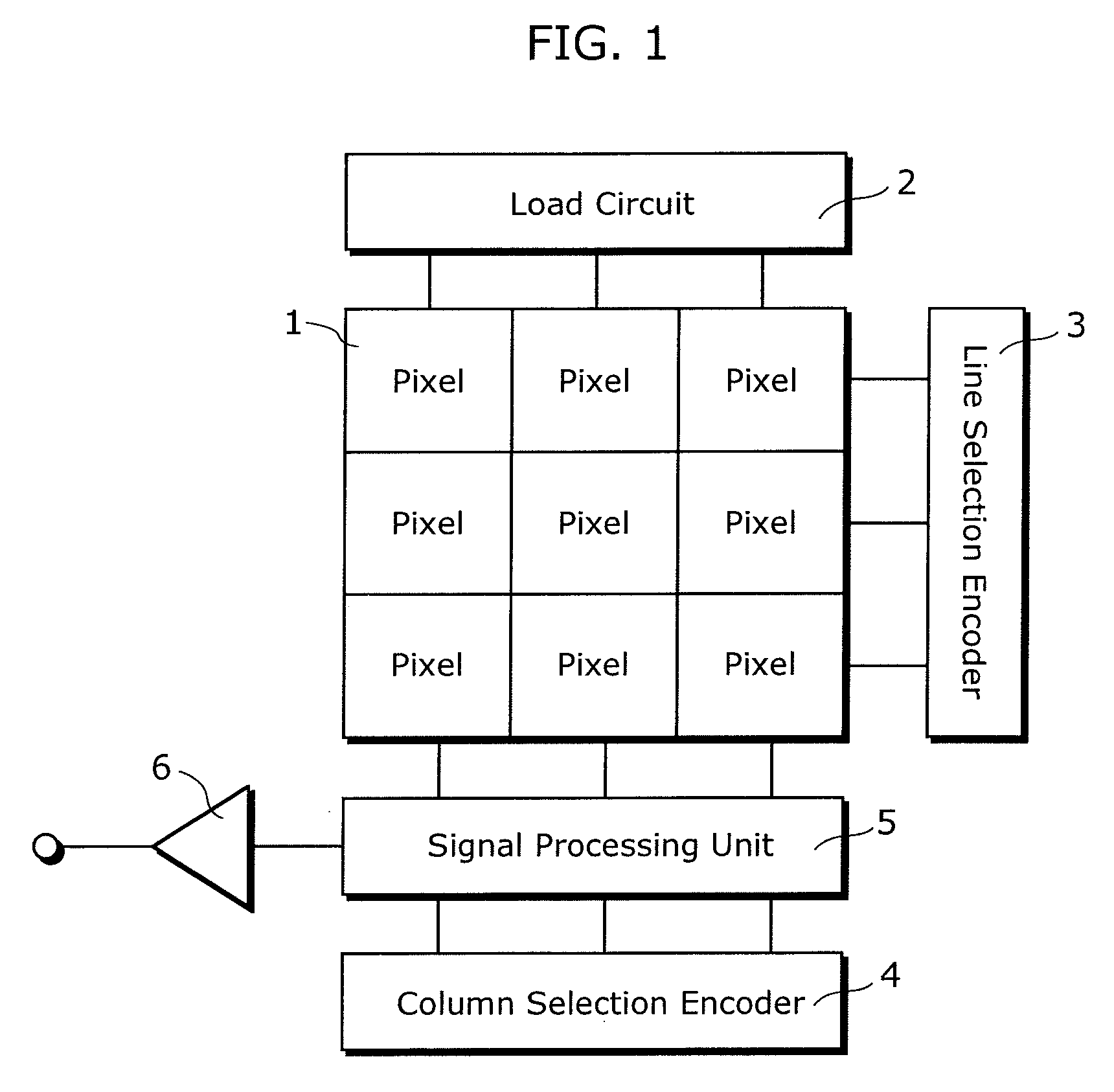
[0048]FIG. 1 is a diagram showing an overall configuration of a solid-state imaging device according to the first embodiment of the present invention.

[0049]The solid-state imaging device is an amplifier-type image sensor which has a function for outputting luminance signals in accordance with the amount of received light, and for avoiding the abovementioned black-crush phenomenon. The solid-state imaging device in configured of an imaging unit 1, a load circuit 2, a line selection encoder 3, a column selection encoder 4, a signal processing unit 5, and an output circuit 6.

[0050]The imaging unit 1 is an imaging region made up of plural pixel circuits (unit cells) arranged either one- or two-dimensionally, and includes a photoelectric conversion unit which converts light to an electric signal. Each pixel circuit outputs a reset voltage, which is a voltage when the photoelectric conversion unit is reset, and a read voltage, which is a voltage arising due to photoelectric conversion per...

second embodiment

[0095]Next, a second embodiment of the present invention shall be described. The present second embodiment is identical to the first embodiment, with the exception of the configuration of the high-intensity judgment circuit. Only the points in which the present embodiment differs from the first embodiment shall be described hereafter.

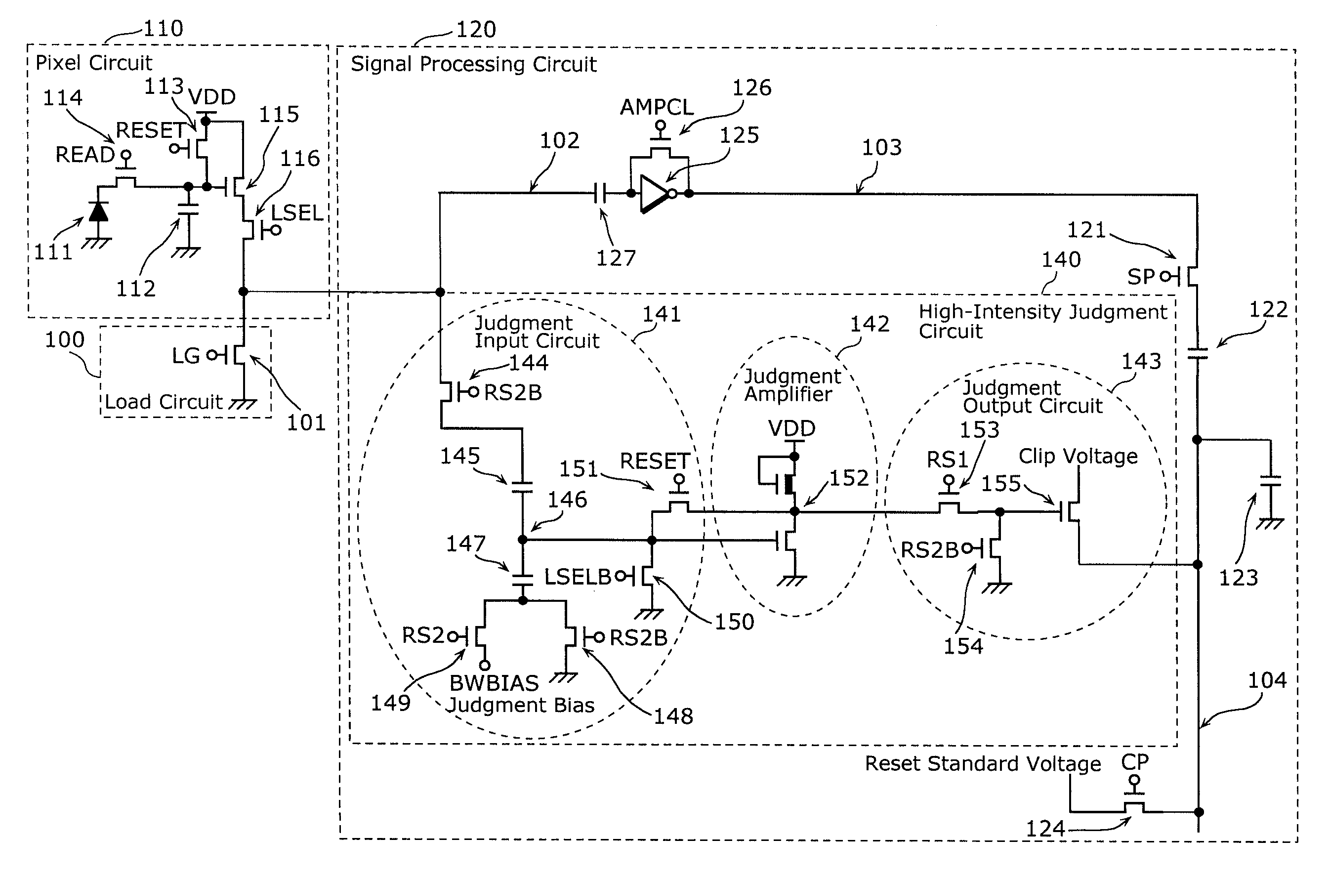
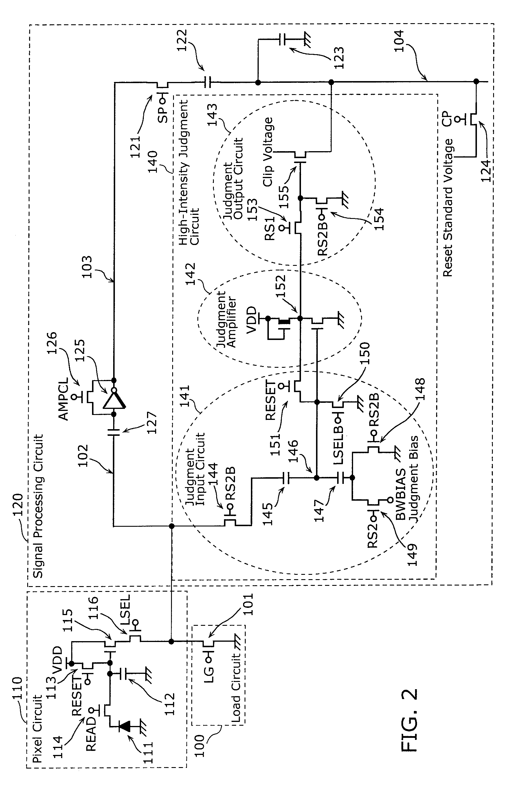
[0096]FIG. 6 is a detailed schematic focusing on one pixel in the solid-state imaging device of the present embodiment. This schematic shows a load circuit 100, a pixel circuit 110, and a signal processing circuit 120 (which includes an intensity detection circuit 140a). Most of these circuits are configured of NMOS transistors; however, some of the circuits (a judgment amplifier 142a) include a PMOS transistor (in other words, are configured of a CMOS).

[0097]The high-intensity judgment circuit 140a is configured of a judgment input circuit 141, the judgment amplifier 142a, and a judgment output circuit 143.

[0098]As opposed to the first embodiment, a ju...

third embodiment

[0111]Next, a third embodiment of the present invention shall be described. The present third embodiment features the same circuit configuration as that of the second embodiment; however, the driving timing of the solid-state imaging device differs from that of the second embodiment. Only the points in which the present embodiment differs from the second embodiment shall be described hereafter.

[0112]In the second embodiment, judgment of whether the light entering the device is in the normal state or the high-intensity state is performed after a difference signal indicating the difference between the reset potential (the potential of the capacitor 112 in timing B) and the read potential (the potential of the capacitor 112 in timing C) is accumulated in the sampling capacitor 123. However, in the present third embodiment, judgment of whether the light entering the device is in the normal state or the high-intensity state is performed simultaneously with the accumulation of the differe...


PUM


Abstract

A solid-state imaging device which can, in response to the problem of black-crush occurring in an image when strong light is enters the device, positively detect black-crush in a state in which a variance margin has been secured. The solid-state imaging device outputs a luminance signal in accordance with an amount of received light, and includes: a pixel circuit having a light-receiving element; a signal output circuit having a sampling transistor which outputs, from a second signal output line, a luminance signal in accordance with the amount of light received by the light-receiving element, based on an output signal from the pixel circuit; and a high-intensity judgment circuit which is coupled by the pixel circuit and a judgment input coupling capacitor, judges whether or not light entering the light-receiving element is of high intensity based on the output signal from the pixel circuit, and in the case of judging the entering light to be of high intensity, outputs a luminance signal indicating high intensity.

Description

BACKGROUND OF THE INVENTION[0001](1) Field of the Invention[0002]The present invention relates to a solid-state imaging device that outputs a luminance signal in accordance with an amount of received light, and in particular to a solid-state imaging device, camera, and driving method for a solid-state imaging device that prevents the occurrence of black-crush in an image when strong light enters the device.[0003](2) Description of the Related Art[0004]Recently, imaging devices which utilize solid-state imaging devices, such as consumer video cameras and digital cameras, have become common. Among such imaging devices, there are devices which employ amplifier-type image sensors as the solid-state imaging device.[0005]While amplifier-type image sensors have excellent features such as low noise levels, they have a problem in that black-crush occurs in images when strong light enters the sensors. “Black-crush” refers to the phenomenon where, due to strong light, electric charge overflows...

Claims


Application Information

Patent Timeline
Patent Type & Authority Applications(United States)
IPC IPC(8): H04N5/217H01L27/146H04N5/335H04N5/355H04N5/369H04N5/374H04N5/3745H04N5/378
CPCH04N5/3598H04N25/627H01L27/146
Inventor TOYA, HIROSHIFUJIOKA, TAKASHIMASUYAMA, MASAYUKIINAGAKI, MAKOTO
Owner COLLABO INNOVATIONS INC
Why Eureka
Try Eureka