Production method for semiconductor device

a production method and semiconductor technology, applied in the direction of semiconductor devices, electrical equipment, basic electric elements, etc., can solve the problems of increasing the number of production process steps, increasing production costs, and disadvantageous roughening of the front surface so as to achieve advantageously prevent contamination of the silicon carbide semiconductor substrate with impurities, the effect of high purity

Active Publication Date: 2007-07-19
ROHM CO LTD
View PDF6 Cites 18 Cited by
  • Summary
  • Abstract
  • Description
  • Claims
  • Application Information

AI Technical Summary

Benefits of technology

[0018] The susceptor preferably has a surface coated by high purity carbon CVD or the like. With this arrangement, the silicon carbide semiconductor substrate can be brought into more intimate contact with the susceptor, and contamination of the silicon carbide semiconductor substrate with impurities can be advantageously prevented.

Problems solved by technology

As a result, the crystalline structure of SiC is changed, so that the front surface of the silicon carbide semiconductor substrate is disadvantageously roughened.
Therefore, the front surface of the silicon carbide semiconductor substrate is liable to be roughened, whichever of the silicon carbide semiconductor substrate and the silicon carbide cap has a higher temperature.
However, the proposed method is disadvantageous in that the protective film should be removed by plasma etching or the like after the annealing, increasing the number of production process steps and the production costs.

Method used


Image

  • Production method for semiconductor device
  • Production method for semiconductor device
  • Production method for semiconductor device

Examples


first embodiment

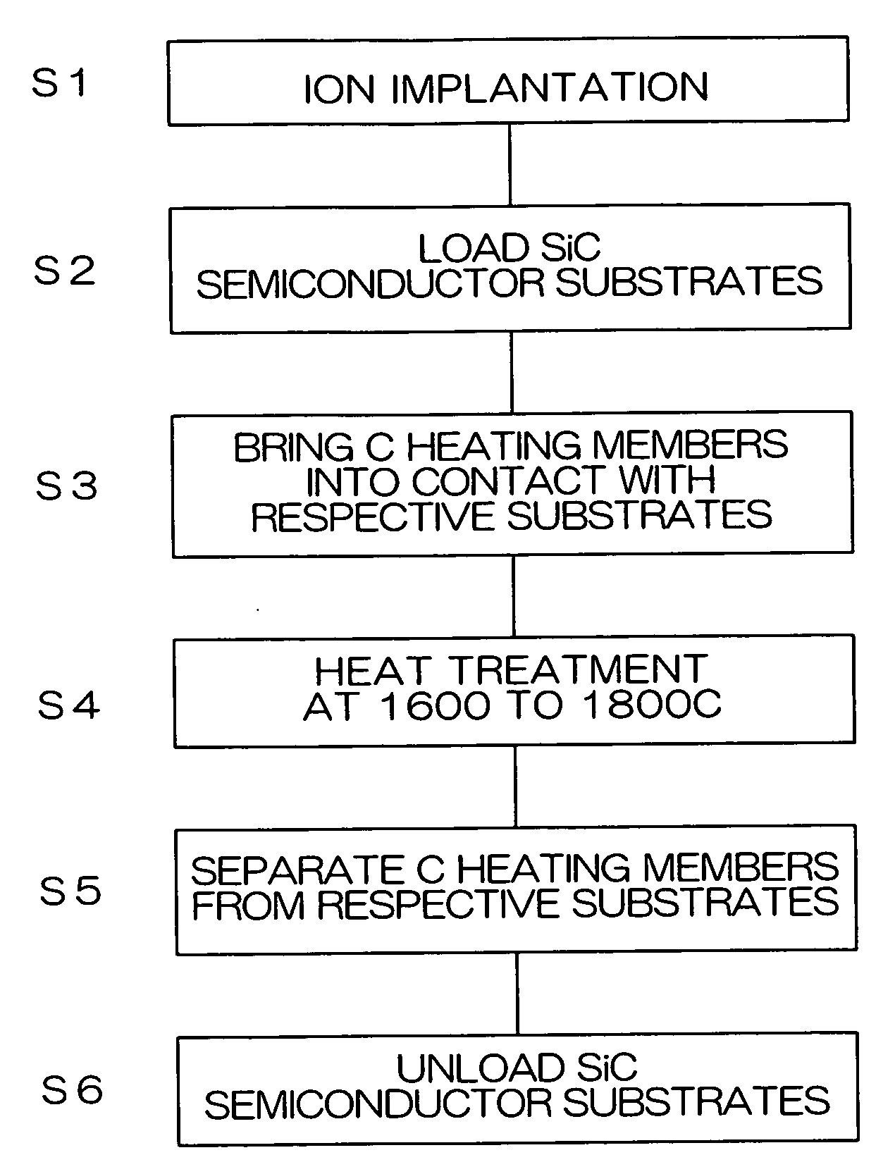
[0023]FIG. 1 is a flowchart showing a process sequence included in a semiconductor device production method according to the present invention.

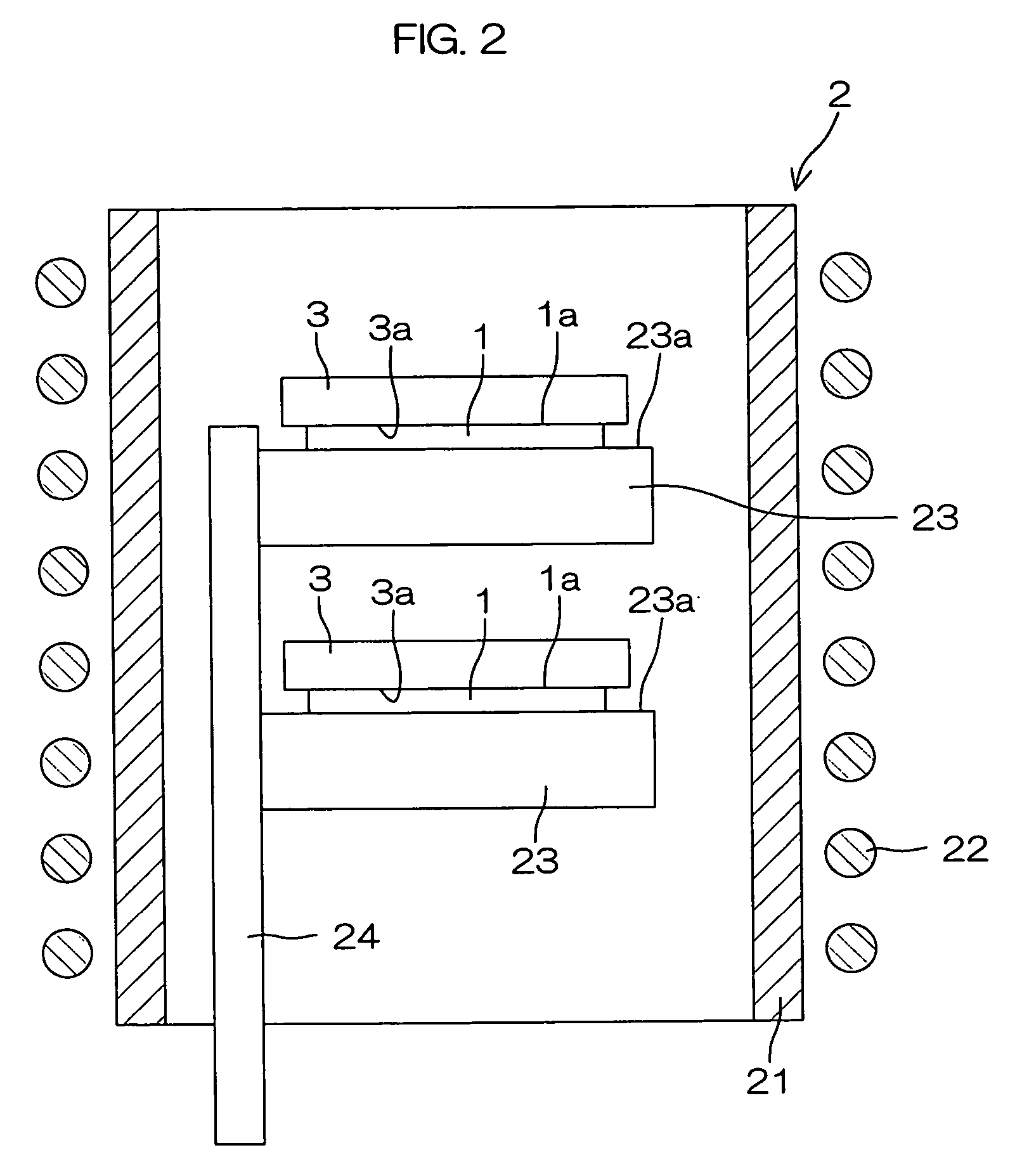
[0024]FIG. 2 is a conceptual sectional view for explaining the production method.

[0025] This production method is a method for forming an impurity region in a front surface (device formation surface) 1a of an SiC semiconductor substrate 1, and is implemented with the use of a high frequency induction oven 2 for annealing (heat-treating) the SiC semiconductor substrates 1 each ion-implanted with an impurity element.

[0026] As shown in FIG. 2, the high frequency induction oven 2 includes a quartz tube 21 having a cylindrical peripheral surface, a high frequency induction heating coil 22 wound around the outer peripheral surface of the quartz tube 21, and a plurality of susceptors 23 each formed of carbon such as graphite. The quartz tube 21 is disposed with its center axis extending generally vertically. The plurality of susceptors 23 are atta...

second embodiment

[0036]FIG. 3 is a conceptual sectional view for explaining a production method according to the present invention. In the production method according to this embodiment, the SiC semiconductor substrates 1 are respectively mounted on the upper surfaces 23a of the susceptors 23 with the front surfaces 1a thereof facing down, and annealed in an inert gas atmosphere or in vacuum.

[0037] The method according to this embodiment also suppresses the roughening of the front surfaces 1a of the SiC semiconductor substrates 1 without increase in the number of production process steps. That is, the temperatures of the susceptors 23 in contact with the front surfaces 1a of the SiC semiconductor substrates 1 are higher than the temperatures of the SiC semiconductor substrates 1 in the annealing, so that the sublimation of Si atoms from the front surfaces 1a of the SiC semiconductor substrates 1 to the susceptors 23 does not occur. Since carbon of the susceptors 23 does not melt at a temperature low...


PUM

PropertyMeasurementUnit
temperatureaaaaaaaaaa
temperaturesaaaaaaaaaa

Abstract

In a production process for a semiconductor device employing an SiC semiconductor substrate (1), the SiC semiconductor substrate (1) is mounted on a susceptor (23), and a C heating member (3) of carbon is placed on a surface of the SiC semiconductor substrate (1). An annealing process is performed to form an impurity region in the surface of the SiC semiconductor substrate (1) by causing the susceptor (23) and the C heating member (3) to generate heat at high temperatures.

Description

BACKGROUND OF THE INVENTION [0001] 1. Field of the Invention [0002] The present invention relates to a production method for a semiconductor device employing a silicon carbide semiconductor substrate. [0003] 2. Description of Related Art [0004] In a production process for a semiconductor device employing a silicon carbide (SiC) semiconductor substrate, an impurity region is formed in a surface of the silicon carbide semiconductor substrate by performing ion implantation and then annealing (heat treatment). [0005] The annealing after the ion implantation is achieved, for example, by mounting the ion-implanted silicon carbide semiconductor substrate on a susceptor of graphite disposed in a quartz tube with the front surface (device formation surface) of the substrate facing up and, in this state, causing the susceptor to generate heat through high frequency induction heating by supplying high frequency power to a coil wound around the outer periphery of the quartz tube. The temperatur...

Claims


Application Information

Patent Timeline
Patent Type & Authority Applications(United States)
IPC IPC(8): H01L21/31H01L21/265H01L21/00H01L21/04H01L21/324H01L29/24
CPCH01L21/0445H01L29/1608H01L21/67103H01L21/324H01L21/265H01L21/425
Inventor MIURA, MINEO
Owner ROHM CO LTD
Why Eureka
Try Eureka