Solar cell

a solar cell and film backheterojunction technology, applied in the field of thin film backheterojunction, can solve the problems of reducing the photogeneration of electron-hole pairs in the active silicon layer of the device, reducing the series resistance, and reducing the size of electrical contacts and buses on the front surfa

Inactive Publication Date: 2007-07-26
KHERANI NAZIR P +1
View PDF17 Cites 175 Cited by
  • Summary
  • Abstract
  • Description
  • Claims
  • Application Information

AI Technical Summary

Benefits of technology

[0009] The present invention describes a novel heterojunction solar cell having thin film amorphous silicon—crystalline silicon back heterojunction and back surface field device configuration prepared at low temperatures. In contrast to present day back junction devices, the back heterojunction device is fabricated by employing low cost processes. These include deposition of thin film layers at low temperature and deployment of low resolution mechanical / shadow masking / lithography. The low temperature of fabrication favours the use of thin silicon wafers. The configuration achieves separation of optimization requirements for efficient light absorption and carrier generation at the front and in the bulk, as well as charge carrier collection at the back.

Problems solved by technology

There are several drawbacks to the prior art silicon photovoltaic devices, namely the front surface of the device that includes electrodes which block and absorb light, preventing it from reaching the underlying active silicon layer and thereby reducing the photogeneration of electron-hole pairs in the active silicon layer of the device.
The presence of the electrical contacts on the front surface makes it problematic for applying an optimal antireflection layer on the front surface, since with the electrical contacts on the front surface they need to be both optically transmissive and electrically conductive.
Further, since the contacts are in the path of the incident light, the electrical contacts and buses on the front surface cannot be significantly increased in size in order to further reduce the series resistance.
With the trend favouring the use of thin silicon wafers, these high temperature processes would lead to thermal damage.
Also, use of high temperature processing increases the cost of processing and thus the cost of the device.
In addition, these back contact photovoltaic devices invariably require high resolution photolithography and associated semiconductor processing.
The presence of the electrical contacts on the front surface makes it problematic for applying an optimal antireflection layer on the front surface, since with the electrical contacts on the front surface they need to be both optically transmissive and electrically conductive.
Further, since the contacts are in the path of the incident light, the electrical contacts and buses on the front surface cannot be significantly increased in size in order to further reduce the series resistance.

Method used


Image

  • Solar cell
  • Solar cell
  • Solar cell

Examples


Embodiment Construction

[0021] The present invention provides a novel low-temperature, thin film back-heterojunction, amorphous-crystalline silicon photovoltaic device. The device disclosed herein is a departure and an improvement over the existing art of back-contact photovoltaic devices as well as heterojunction photovoltaic devices. The device disclosed herein uses low temperature thin film back-heterojunctions which are prepared by low temperature deposition of undoped and doped amorphous silicon on crystalline silicon, in contrast to the high temperature diffused back junctions in existing devices.

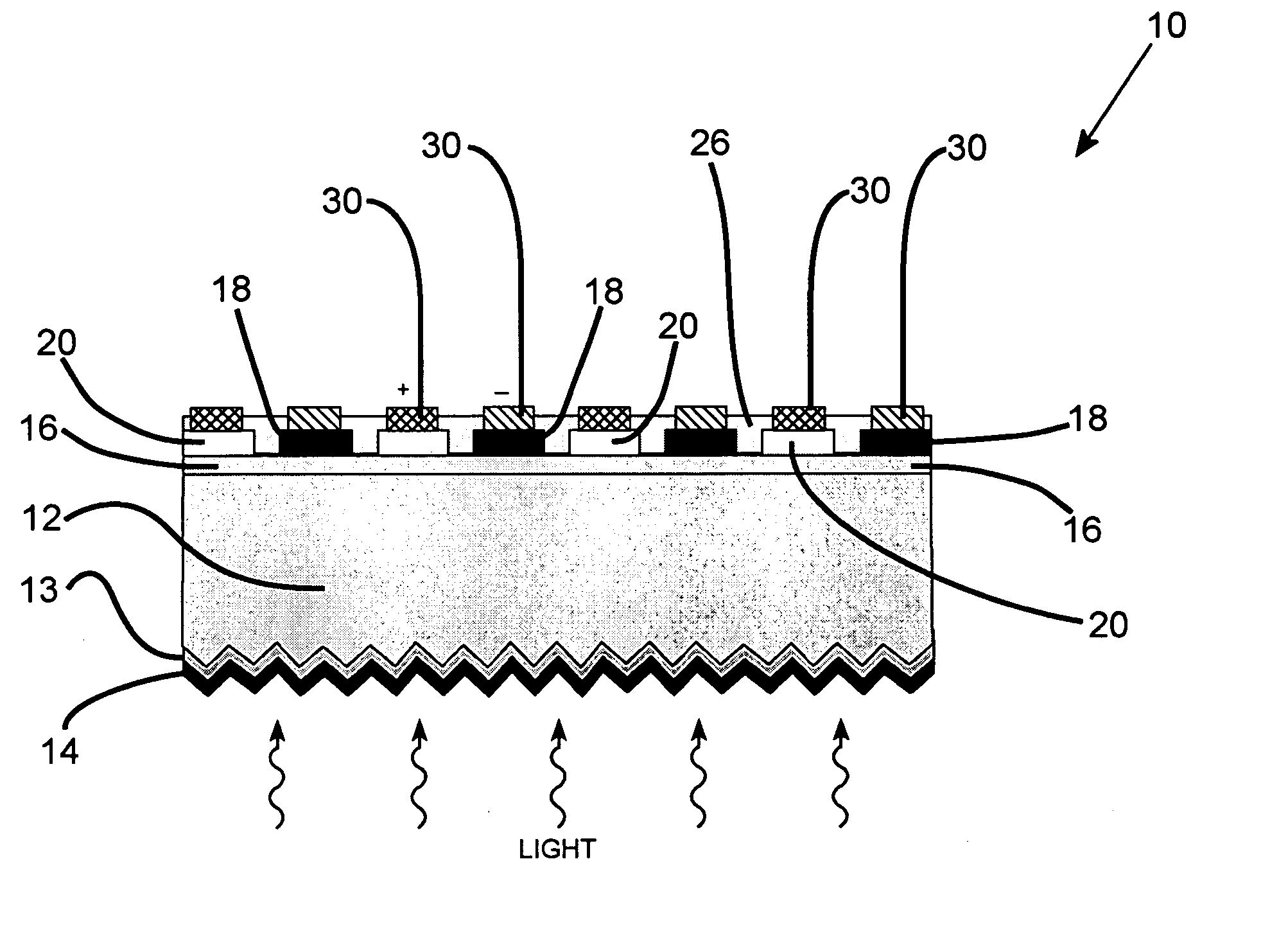
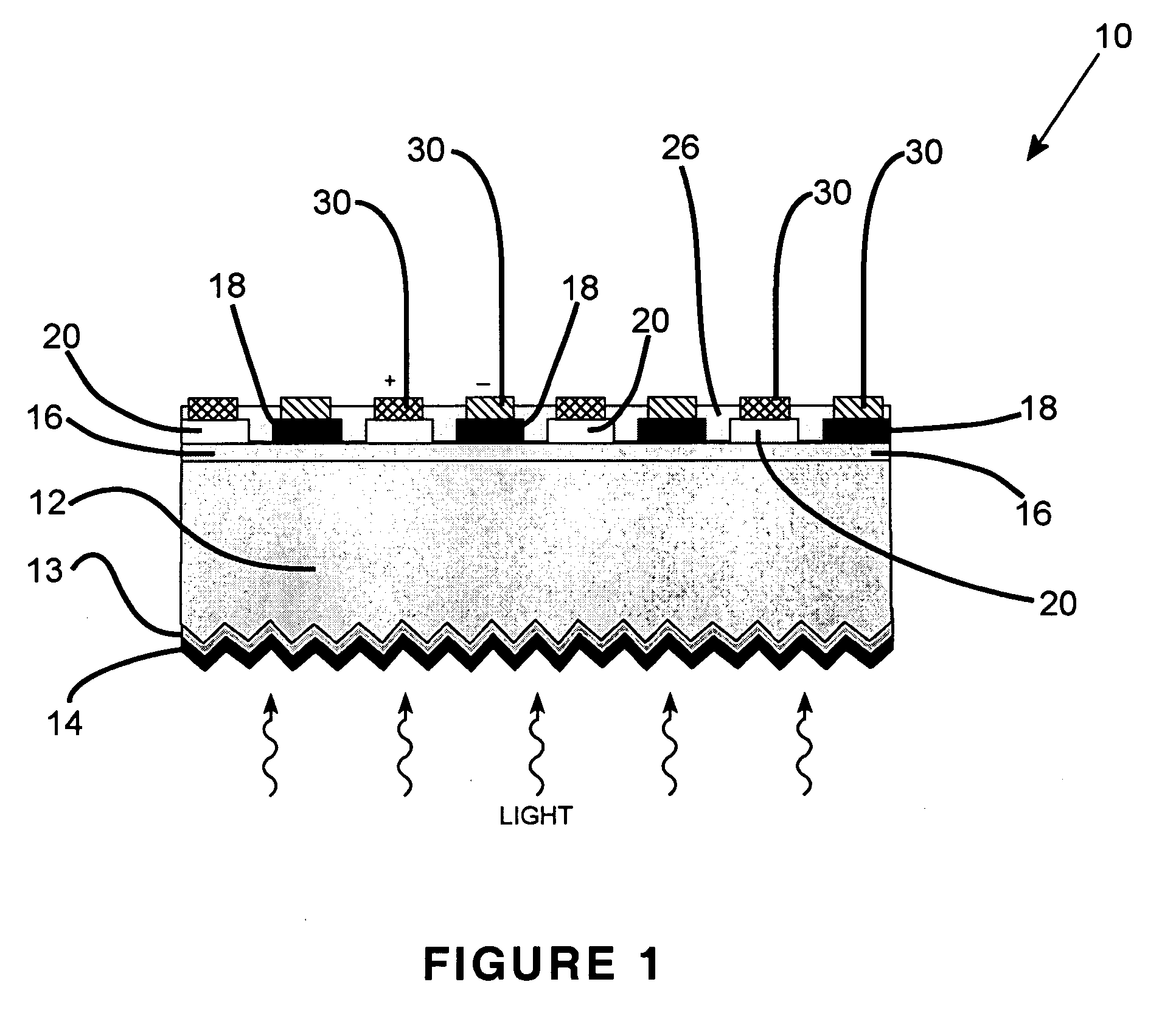
[0022] Referring first to FIG. 1, a thin film back-heterojunction, amorphous-crystalline silicon photovoltaic device shown generally at 10 includes a crystalline silicon wafer 12 which may have a thickness in a range from about 100 μm to about 300 μm.

[0023] The front surface of the crystalline silicon wafer 12, which is often textured for light trapping, usually includes a passivating layer 13 and / or an an...


PUM

PropertyMeasurementUnit
temperaturesaaaaaaaaaa
thicknessaaaaaaaaaa
temperatureaaaaaaaaaa

Abstract

The present invention provides a thin film amorphous silicon-crystalline silicon back heterojunction and back surface field device configuration for a heterojunction solar cell. The configuration is attained by the formation of heterojunctions on the back surface of crystalline silicon at low temperatures. Low temperature fabrication allows for the application of low resolution lithography and/or shadow masking processes to produce the structures. The heterojunctions and interface passivation can be formed through a variety of material compositions and deposition processes, including appropriate surface restructing techniques. The configuration achieves separation of optimization requirements for light absorption and carrier generation at the front surface on which the light is incident, and in the bulk, and charge carrier collection at the back of the device. The shadowing losses are eliminated by positioning the electrical contacts at the back thereby removing them from the path of the incident light. Back contacts need optimization only for maximum charge carrier collection without bothering about shading losses. A range of elements/alloys may be used to effect band-bending. All of the above features result in a very high efficiency solar cell. The open circuit voltage of the back heterojunction device is higher than that of an all-crystalline device. The solar cell configurations are equally amenable to crystalline silicon wafer absorber as well as thin silicon layers formed by using a variety of fabrication processes. The configurations can be used for radiovoltaic and electron-voltaic energy conversion devices.

Description

FIELD OF THE INVENTION [0001] The present invention relates to thin film back-heterojunction, amorphous-crystalline silicon photovoltaic devices produced at low-temperatures. BACKGROUND OF THE INVENTION [0002] Most of the present day silicon photovoltaic devices are configured so that a p-n junction is formed in silicon by diffusion of dopants at elevated temperatures and the application of electrodes on the light facing side and back-side. Back contacts on silicon photovoltaic devices are formed, using high temperature processing, to substantially overcome the shading losses on the light facing side. Amorphous-crystalline silicon heterojunction photovoltaic devices are formed by the deposition of amorphous silicon layers on crystalline silicon, thereby substantially providing for low temperature processing. In this case, the electrodes are applied on the light facing front side as well as back-side of the device. [0003] JP 18413358 to Hamakawa et al., and U.S. Pat. No. 4,496,788 di...

Claims


Application Information

Patent Timeline
Patent Type & Authority Applications(United States)
IPC IPC(8): H01L31/00
CPCH01L31/0745H01L31/077H01L31/02167H01L31/022441H01L31/0747Y02E10/50Y02E10/547
Inventor KHERANI, NAZIR PYARALIRAYAPROL, BHANU GANGADHARYEGHIKYAN, DAVITZUKOTYNSKI, STEFAN
Owner KHERANI NAZIR P
Why Eureka
Try Eureka