Thin film organic position sensitive detectors

a position sensitive, organic technology, applied in thermoelectric devices, instruments, radio frequency controlled devices, etc., can solve the problems of inability to continuously detect signals, difficult and expensive production, and difficult to produce high-efficiency crystalline devices, etc., to achieve enhanced response time, high detection resolution, and increased potential barriers

Inactive Publication Date: 2007-08-02
FORREST STEPHEN R +2
View PDF49 Cites 199 Cited by
  • Summary
  • Abstract
  • Description
  • Claims
  • Application Information

AI Technical Summary

Problems solved by technology

However, efficient crystalline-based devices, especially of large surface area, are difficult and expensive to produce due to the problems inherent in producing large crystals without significant efficiency-degrading defects.
On the other hand, high efficiency amorphous silicon devices still suffer from problems with stability.
A disadvantage of this configuration is the inability to continuously detect a signal without their resolution being limited by detector size.
The a-Si:H films are advantageous over previously used crystalline silicon since they can be made at lower cost and with higher surface area than the crystalline PSDs, however, the size limitation and fabrication cost of a-Si:H films still substantially limits the usefulness of silicon-based PSDs.
However, this device is limited to having a single biological material that must be buffered with a high pH, and has a low spatial resolution (approximately +1 mm error) which decreases with increased width of the detector which make this device unusable for many applications.

Method used


Image

  • Thin film organic position sensitive detectors
  • Thin film organic position sensitive detectors
  • Thin film organic position sensitive detectors

Examples


example 1

ication

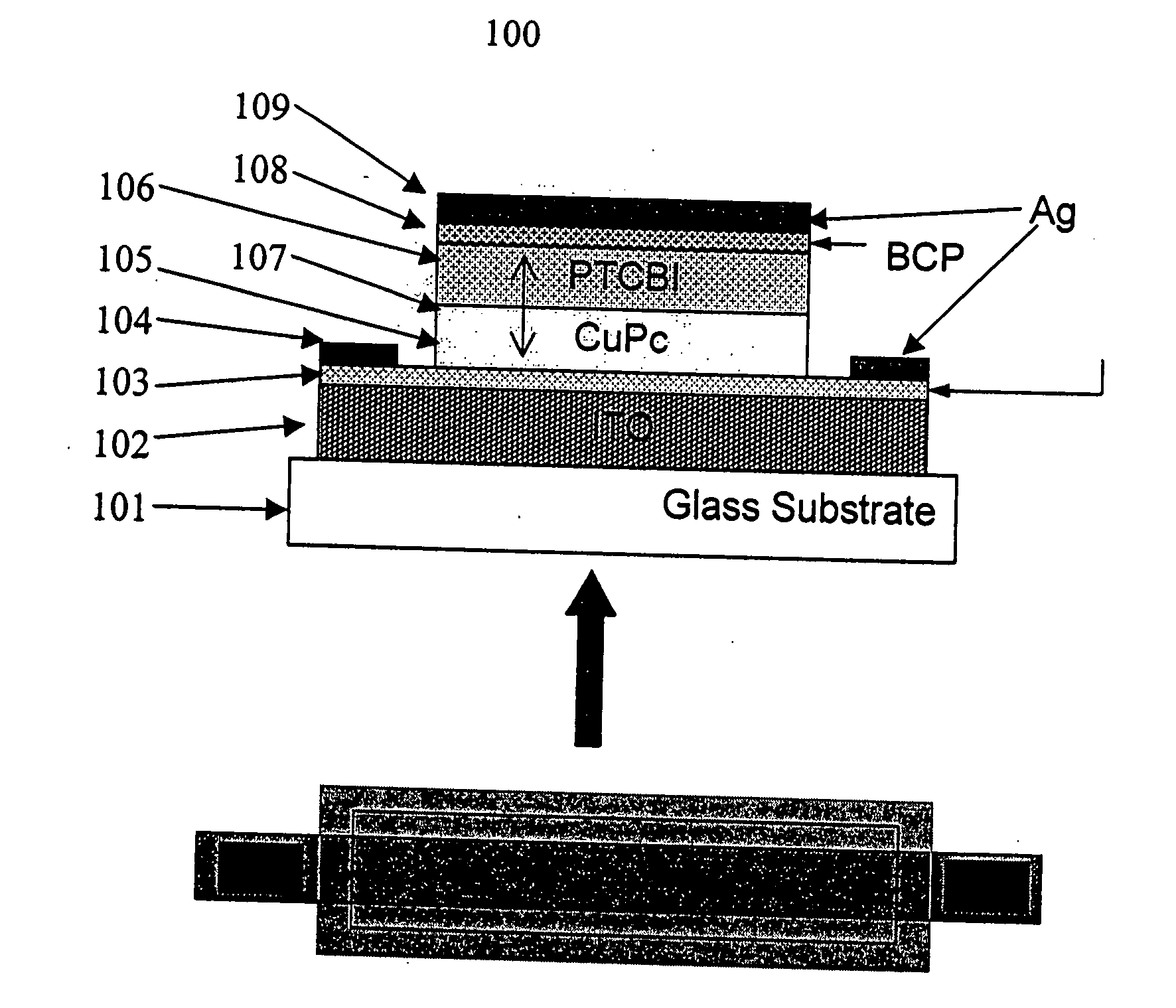
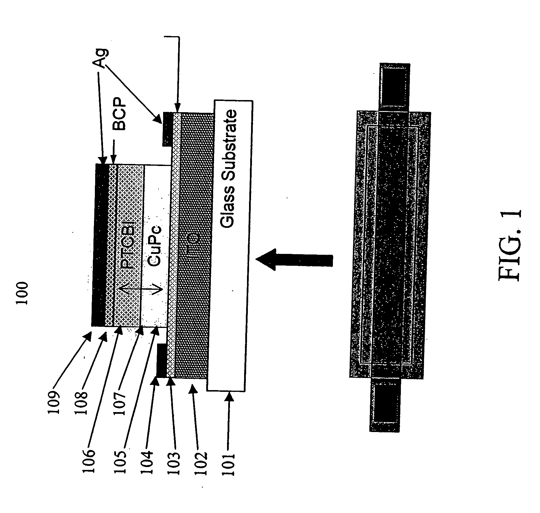
[0074] An OPSD was fabricated on precleaned glass substrates commercially precoated with a 1500 Å-thick ITO anode obtained from Applied Films Corporation in Longmont Colo. (P. E. Burrows, Z. Shen, V. Bulovic, D. M. McCarty, S. R. Forrest, J. A. Cronin, and M. E. Thompson, “Relationship between electroluminescence and current transport in organic hetero-junction light-emitting devices,” J. Appl. Phys., vol. 79, no. 10, pp. 7991-8006, May 1996.) A single photolithographic step was used to pattern and etch the ITO (in 5% HNO3: 45% HCl: 50% H2O by volume at 70° C. for 5 min) into a 3 cm×1 mm line. The ITO was then spin-coated with a 300 Å-thick film of 3,4-polyethylenedioxythiophene:polystyrenesulfonate (PEDOT:PSS), followed by drying at 120° C. for 15 min in vacuum. The PEDOT:PSS layer improves current injection into the donor-like copper phthalocyanine (CuPc) layer by lowering the Fermi-level, and hence reducing the energy barrier to holes by 0.5 eV with the highest occupied mo...

example 2

ng the Electronic and Optical Characteristics of the OPSD

[0075]FIG. 4 shows the current density-versus-voltage characteristics for the OPSD in the dark and under different intensities at a wavelength of λ=632.8 nm using a HeNe laser. The signal-to-background ratio (SBR) can be defined as Iph / ID, where Iph is the photocurrent and ID is the dark current of the device. A minimum SBR of 9 satisfies the condition IDph such that the OPSD response is linear and thus leads to an accurate determination of Δx. In particularly preferred embodiments, SBRs>1000 are achieved at low reverse bias for optical powers>500 μW.

[0076] The absorption (solid line) and external quantum efficiencies (ηEXT) for different applied voltages (dashed lines) are shown in FIG. 5. The absorption has three peaks at λ=550, 610, and 680 rim. The λ=550 nm peak is due to the PTCBI layer while CuPc is responsible for the shoulder at λ=610 nm and the peak at λ=680 nm. Note that ηEXT differs from the absorption spectrum sin...

example 3

of the OPSD

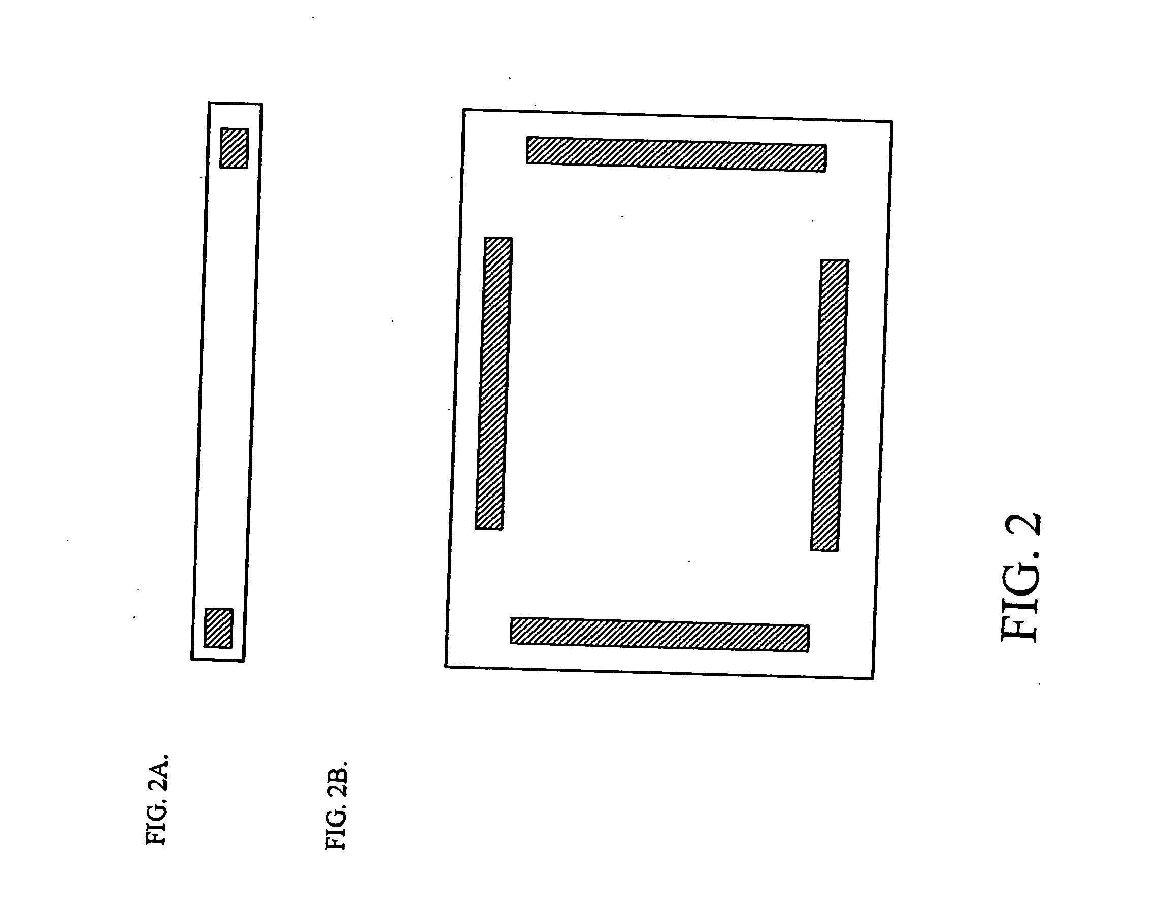
[0077] All 3 cm×1 mm OPSDs were scanned using a translation stage accurate to less than 10 μm and an optical beam of diameter 180 μm. To characterize beam tracking accuracy, the nonlinearity factor, δ=2σ / F was used, where σ is the root mean square deviation from a regression line fit to the measured position, and F is the full positional range of the data. Typically, δ<0.15 is sufficient for many applications. (E. Fortunato, G. Lavareda, R. Martins, F. Soares, and L. Fernandes, “Large-area 1 D thin-film position-sensitive detector with high detection resolution,” Sensor Actuat. A: Phys., vol. 51, no. 2-3, pp. 135-142, February 1996.) Another important parameter for the OPSD is the measurement error, Σ=(ΔI / L) where Δ1 is the difference between the actual and calculated optical beam positions. (S. Arimoto, H. Yamamoto, H. Ohno, and H. Hasegawa, “Hydrogenated amorphous silicon position sensitive detector,” J. Appl. Phys., vol. 57, no. 10, pp. 4778-4782, May 1985.) In FIG. 7,...


PUM

PropertyMeasurementUnit
poweraaaaaaaaaa
widthaaaaaaaaaa
work functionaaaaaaaaaa

Abstract

The present invention is directed to organic photosensitive optoelectronic devices and methods of use for determining the position of a light source. Provided is an organic position sensitive detector (OPSD) comprising: a first electrode, which is resistive and may be either an anode or a cathode; a first contact in electrical contact with the first electrode; a second contact in electrical contact with the first electrode; a second electrode disposed near the first electrode; a donor semiconductive organic layer disposed between the first electrode and the second electrode; and an acceptor semiconductive organic layer disposed between the first electrode and the second electrode and adjacent to the donor semiconductive organic layer. A hetero-junction is located between the donor layer and the acceptor layer, and at least one of the donor layer and the acceptor layer is light absorbing. The OPSD has an optical beam spatial resolution of 20 μm and measurements are insensitive to fluctuations in incident light beam intensity and background illumination. The response of the OPSD shows high linearity, low positional error, high spatial resolution, and good beam tracking velocity. The OPSDs exhibited linearities and positional uncertainties of <1%.

Description

[0001] This application is a continuation of U.S. application Ser. No. 10 / 607,211, filed Jun. 25, 2003, which claims priority to Provisional Patent Application Ser. No. 60 / 454,836, filed Mar. 14, 2003, herein incorporated by reference. The contents of those applications are incorporated herein in their entirety by reference.GOVERNMENT RIGHTS [0002] This invention was made with Government support under Contract No. F49620 00 1 0065 awarded by Air Force Office of Scientific Research. The government has certain rights in this invention.RESEARCH AGREEMENTS [0003] The claimed invention was made by, on behalf of, and / or in connection with one or more of the following parties to a joint university corporation research agreement: Princeton University, The University of Southern California, and Universal Display Corporation. The agreement was in effect on and before the date the claimed invention was made, and the claimed invention was made as a result of activities undertaken within the sco...

Claims


Application Information

Patent Timeline
Patent Type & Authority Applications(United States)
IPC IPC(8): H01L29/08H01L27/14H01L31/0232H01J40/14H01L27/30H01L31/00H01L31/101H01L51/00H01L51/42
CPCH01L27/305H01L31/101H01L51/0037H01L51/0053Y02E10/549H01L51/0078H01L51/4246H01L2251/308H01L51/0062G01S7/4816H10K39/30H10K85/1135H10K85/621H10K85/649H10K85/311H10K30/211H10K2102/103
Inventor FORREST, STEPHEN R.RAND, BARRY P.LANGE, MICHAEL J.
Owner FORREST STEPHEN R
Why Eureka
Try Eureka