Alignment mark and overlay inspection mark

a technology of alignment marks and overlays, applied in the direction of instruments, photomechanical devices, optics, etc., can solve the problems of adhesive force between the alignment marks and the surface, deviation of resist patterns, and separation of overlay inspection marks, so as to prevent separation, prevent breakage, and prevent crack generation

Inactive Publication Date: 2007-08-02
LAPIS SEMICON CO LTD
View PDF5 Cites 13 Cited by
  • Summary
  • Abstract
  • Description
  • Claims
  • Application Information

AI Technical Summary

Benefits of technology

[0038]In the above described alignment mark, the lengths of the patterns (along the long axes) are short, and the patterns are separate from each other. In the above described overlay inspection mark, the lengths of the dot marks (along the long axes) are short, and the dot marks are separate from each other. Therefore, even when the upper layer and/or the lower layer (for example, an insulation film) is thermally expanded or shrunk by a heat treatment in the manufacturing process, the stre

Problems solved by technology

However, even when the above described alignment mark is used, if the same resist pattern includes the device pattern and the alignment mark that are different from each other in shape, size, density or the like, the deviation of the resist patterns may occur due to the difference in shape, size, density or the like.
However, the length of the alignment mark in the direction perpendicular to the alignment adjustment direction has not been considered to cause problems, as long as the overlay accuracy required to enable the alignment adjustment can be obtained.
If the alignment mark and the overlay inspection mark are long, the heat treatment may cause the following problems.(1) Th

Method used


Image

  • Alignment mark and overlay inspection mark
  • Alignment mark and overlay inspection mark
  • Alignment mark and overlay inspection mark

Examples


first embodiment

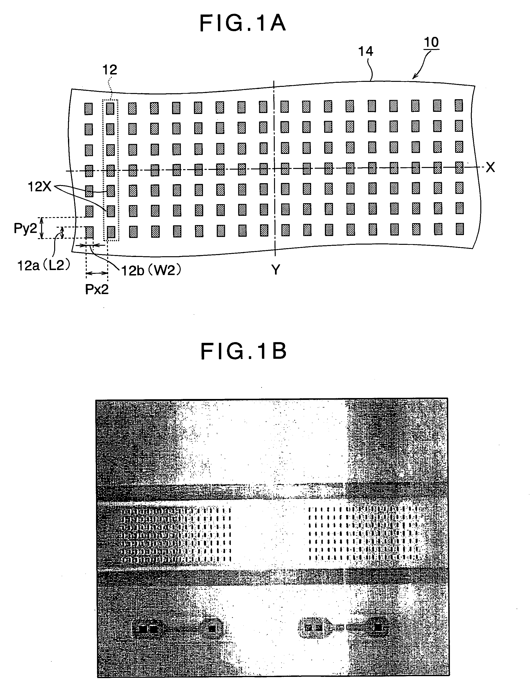
[0053]A configuration example of an alignment mark of the first embodiment of the present invention will be described with reference to FIG. 1. The configuration example is intended to prevent the generation of the crack in the heat treatment. In this example, the alignment mark is formed at the same time as the formation of tungsten (W) plugs so that the alignment mark has the same structure as the tungsten plugs. Therefore, the alignment mark of the first embodiment is particularly suitable for alignment adjustment of a resist mask used after the forming process of the tungsten plugs.

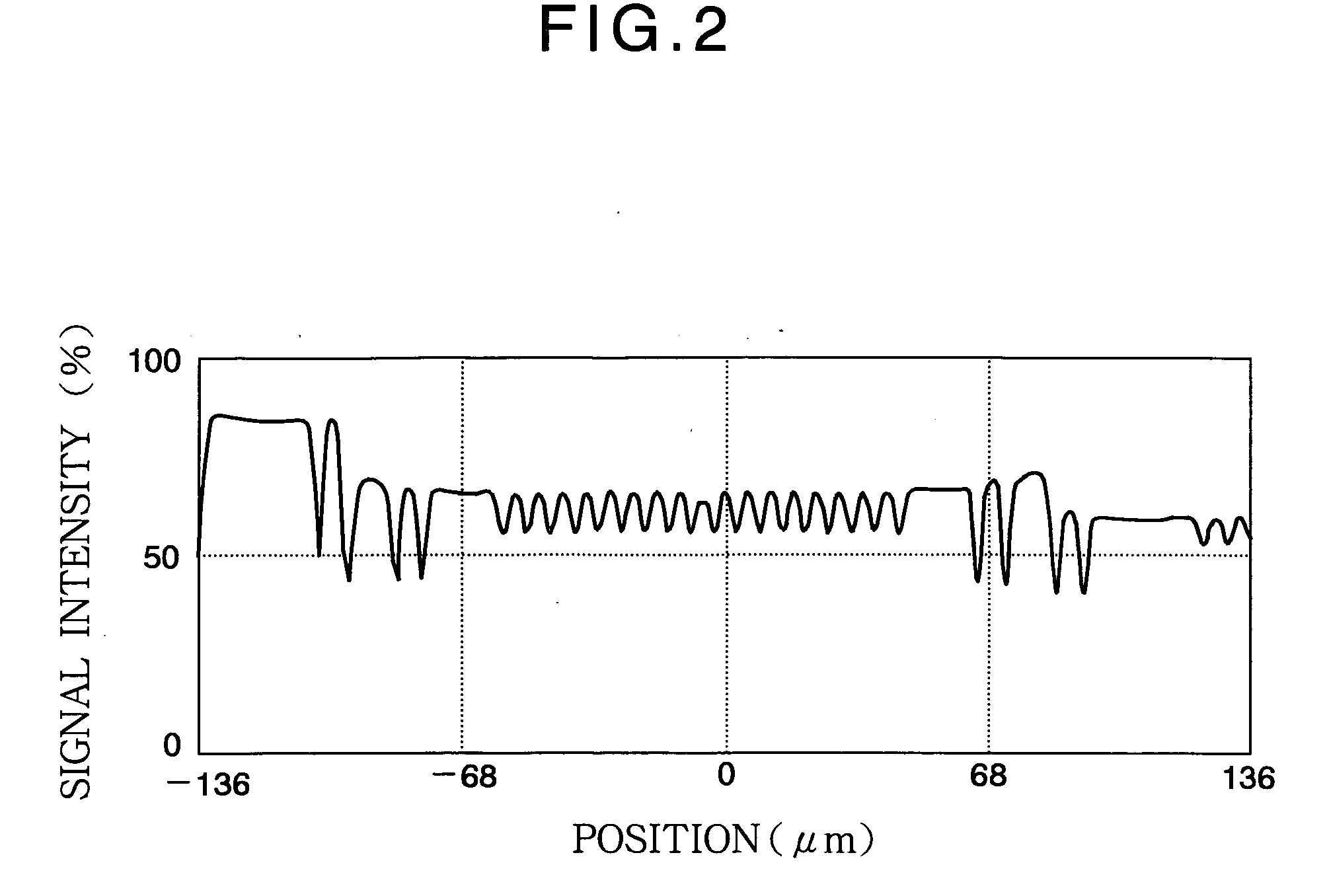
[0054]FIG. 1A is a schematic plan view showing the alignment mark of the first embodiment as seen from above. FIG. 1B is a photographic view of the alignment mark taken by optical microscope at the magnification of 50 times.

[0055]The configuration example of the alignment mark used for the alignment adjustment in the direction of X-axis will be described. The alignment mark 10 includes linear array pa...

second embodiment

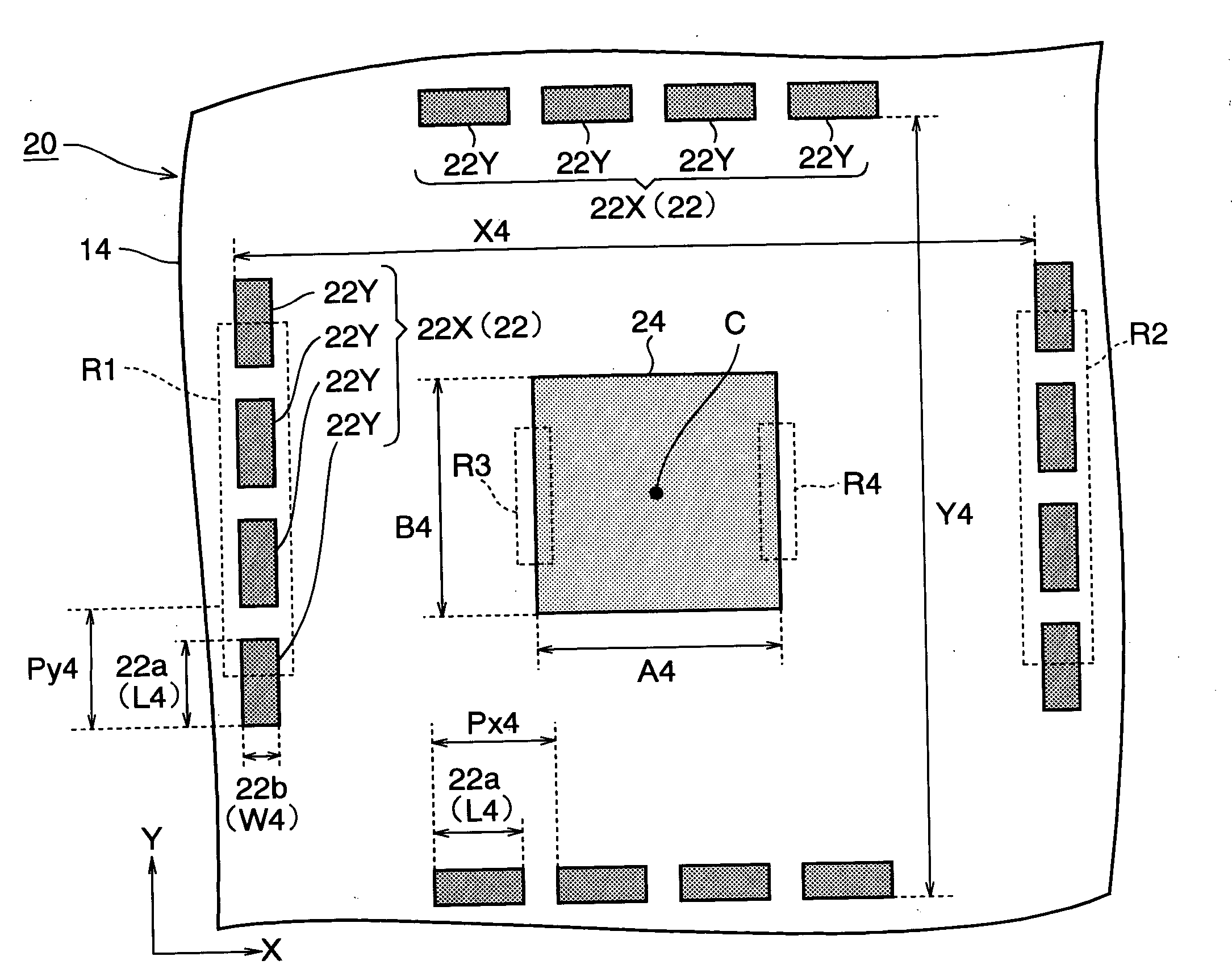
[0096]A configuration example of the alignment mark of the second embodiment will be described with reference to FIG. 5A. The configuration example of the alignment mark is intended to prevent the breakage of the alignment mark due to the heat treatment.

[0097]FIG. 5A is a schematic plan view of the alignment mark of the second embodiment. FIG. 5B is a schematic view of an overlay inspection mark of the second embodiment as seen from above.

[0098]The configuration example of the alignment mark used for the alignment adjustment in the direction of X-axis will be described. The alignment mark 10 is formed at the same time as a ferroelectric capacitor structure in a forming process of the ferroelectric capacitor structure of the ferroelectric memory device. Therefore, the alignment mark 10 of the second embodiment is particularly suitable for alignment adjustment of a resist mask used after the forming process of the ferroelectric capacitor structure.

[0099]As shown in FIG. 5A, the alignm...


PUM


Abstract

An alignment mark is formed on an underlying layer and disposed on a region in which a semiconductor device is not formed. The alignment mark includes a plurality of strip-shaped patterns detectable by an optical imaging device. The patterns have long axes and short axes. The patterns are arranged in a matrix of rows and columns in such a manner that the long axes are substantially perpendicular to the direction of the alignment adjustment.

Description

BACKGROUND OF THE INVENTION[0001]This invention relates to a manufacturing method of a semiconductor device, and particularly relates to an alignment mark and an overlay inspection mark employed in the manufacturing method for enhancing the overlay accuracy of resist patterns (i.e., resist masks) used in a plurality of photolithography processes.[0002]In the manufacturing process of the semiconductor device (i.e., a wafer process), several tens layers of resist patterns are formed by photolithography to manufacture one kind of semiconductor device.[0003]A resist pattern (having a predetermined pattern) is formed by forming a resist layer on the entire surface of a wafer and by patterning the resist layer in an exposing process using an exposing device.[0004]For example, in order to form a second pattern on a first pattern (having been patterned using a first resist pattern), it is necessary to accurately align a second resist-pattern with the first pattern.[0005]Generally, in order ...

Claims


Application Information

Patent Timeline
IPC IPC(8): H01L23/544H01L21/00
CPCG03F7/70633H01L23/544H01L21/67294H01L2924/0002H01L2924/00
Inventor SASAKI, SUGURU
Owner LAPIS SEMICON CO LTD
Why Eureka
Try Eureka