
Semiconductor integrated circuit device

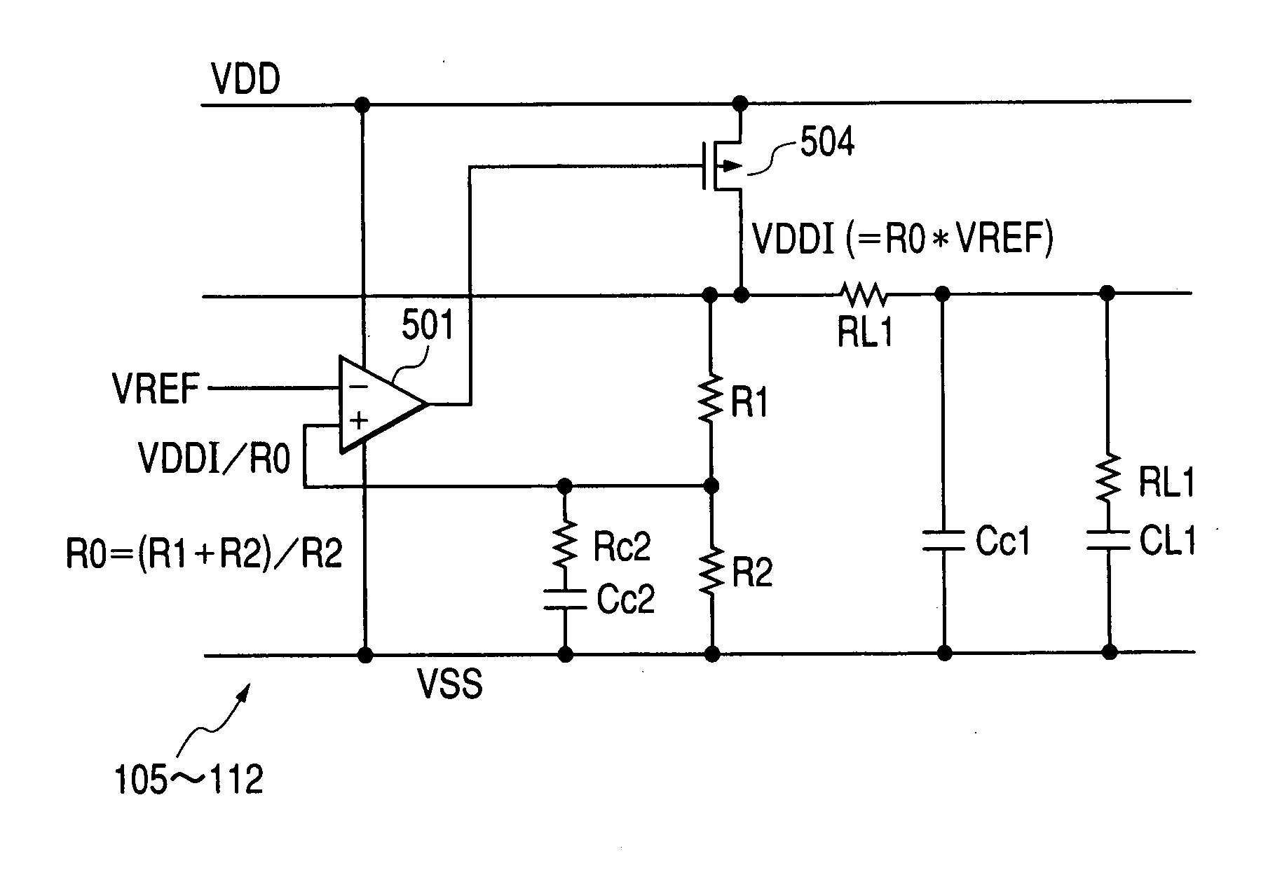
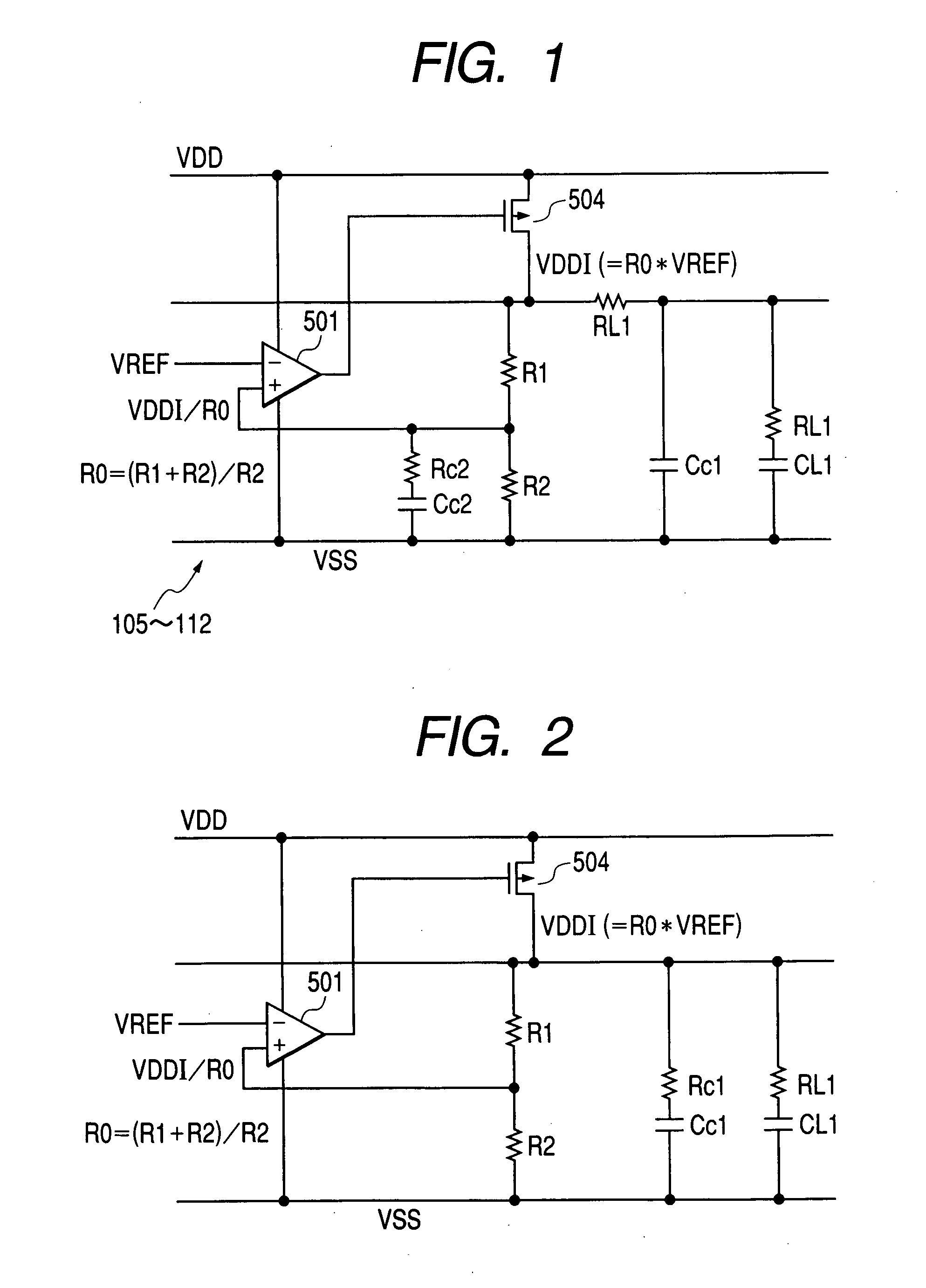
a technology of integrated circuits and semiconductors, which is applied in the direction of dc-coupled stages, differential amplifiers, instruments, etc., can solve the problems of reducing the drain conductance of the driver pmos, hindering appropriate phase compensation, and lowering composite resistance, so as to reduce resistance and capacitance, reduce phase delay, and reduce resistance of metal wiring for internal supply voltage vddi

Inactive Publication Date: 2007-08-02
RENESAS ELECTRONICS CORP
View PDF13 Cites 2 Cited by
  • Summary
  • Abstract
  • Description
  • Claims
  • Application Information

AI Technical Summary

Benefits of technology

This configuration secures a stable phase margin and reduces the chip occupancy area, enabling the use of short gate length transistors and high current consumption without increasing wiring resistance, thus enhancing the reliability and efficiency of the limiter circuit.

Problems solved by technology

However, applying a short gate length to the driver PMOS will decrease the drain conductance of the driver PMOS.
And, the phase compensating resistors connected in series to the individual phase compensating capacitors are mutually connected in parallel to thereby lower the composite resistance, which hinders appropriate phase compensation.
In this manner, when the drain conductance of the driver PMOS is low, it is unavoidable that the chip occupancy area for the phase compensating capacitor and the phase compensating resistor becomes increased in the pole / zero compensation system.
However, there is practically a certain limit in the occupancy area for the phase compensating capacitor and the phase compensating resistor from the restriction of the chip size, which makes it difficult to attain a sufficient phase margin.

Method used


Image

  • Semiconductor integrated circuit device
  • Semiconductor integrated circuit device
  • Semiconductor integrated circuit device

Examples


Embodiment Construction

[0048]FIG. 10 illustrates an SRAM (Static Random Access Memory) as an example of the semiconductor integrated circuit device according to the invention.

[0049] The SRAM 2 is assumed to be a flip-chip type, which is not limited to this. The SRAM 2 has a BGA (Ball Grid Array) substrate connected on a semiconductor chip 20. The semiconductor chip 20 is formed on a semiconductor substrate such as a single crystal silicon substrate by means of the known production technique for the semiconductor integrated circuit.

[0050] The BGA substrate has the BGA balls as the external terminals that permit electrical connections to a component mounting board and so forth. The semiconductor chip 20 and the BGA substrate are electrically connected by way of bump electrodes.

[0051] The semiconductor chip 20 has memory cell arrays 101, 102 formed with two partitions divided in the latitudinal direction. A central circuit area 125 is allocated between the memory cell arrays 101, 102. The memory cell arra...


PUM


Abstract

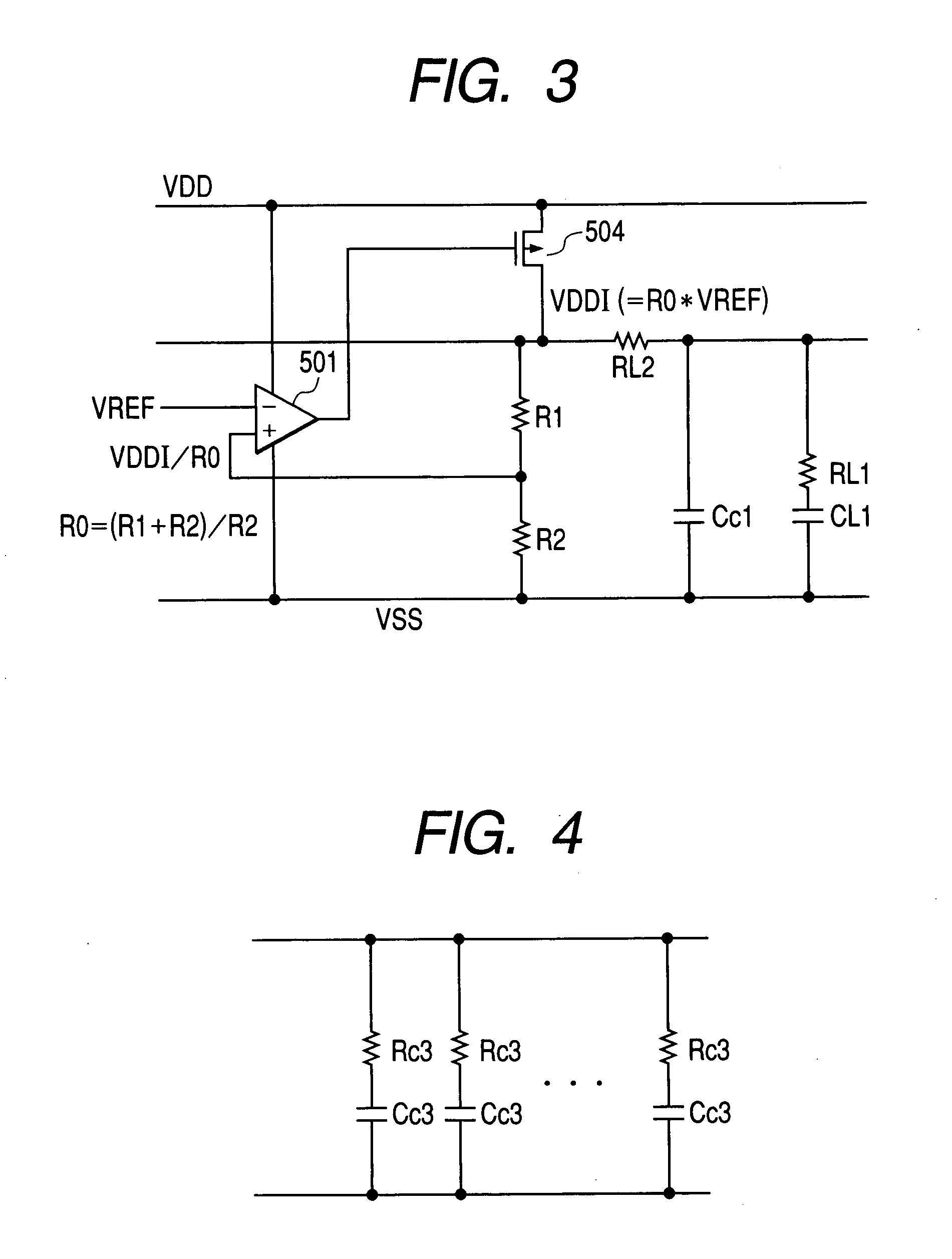
The invention intends to provide a technique that achieves a sufficient phase margin with ease. The circuit includes a power supply circuit that is formed with a phase compensating resistor and a phase compensating capacitor, between a second input terminal of a differential amplifier and a low supply voltage. Thereby, the first pole frequency in the overall gain is determined by the first pole frequency in the voltage-dividing resistor stage in the Bode diagram for the pole / zero compensation, which is shifted to a lower frequency. Also, the zero point cancels the first pole frequency in the differential amplifier stage, which reduces the phase delay to secure the phase margin. And, since the phase compensating resistor can take a considerably high resistance, the same characteristic can be achieved with a low capacitance of the phase compensating capacitor; thereby, the phase compensation becomes possible with a resistor and a capacitor having a smaller size than the pole / zero compensation with the internal supply voltage.

Description

BACKGROUND OF THE INVENTION [0001] The present invention relates to a semiconductor integrated circuit device, more specifically to a phase compensation technique for amplifiers that the circuit device contains. [0002] As a general trend in the semiconductor integrated circuit device, the withstanding voltage is being lowered, accompanied with the advancement of micro fabrication of MOS transistors. Accordingly, when a high supply voltage VDD is supplied from the outside, an internal supply voltage VDDI being lower than VDD is generated on the basis of the high supply voltage VDD, and the internal supply voltage VDDI is supplied to internal circuits as the operational supply voltage. Such an internal supply voltage VDDI is generated by means of a limiter circuit (named also as voltage-dropping circuit). [0003] The limiter circuit includes a p-channel MOS transistor called a driver PMOS, and a differential amplifier that drives the driver PMOS on the basis of the comparison result of...

Claims


Application Information

Patent Timeline
Patent Type & Authority Applications(United States)
IPC IPC(8): G05F1/00H01L27/04G05F1/56H01L21/822H03F3/45
CPCG05F1/56
Inventor TOYOSHIMA, HIROSHINISHIYAMA, MASAHIKO
Owner RENESAS ELECTRONICS CORP
Learn More