Crystallization method for semiconductor film, manufacturing method for semiconductor device, and laser irradiation apparatus

a manufacturing method and semiconductor technology, applied in the direction of laser beam welding apparatus, manufacturing tools, solid-state devices, etc., can solve the problem of increasing manufacturing costs, and achieve the effect of suppressing the generation of in-plane variations in the properties of crystallized semiconductor films and suppressing the generation of variations in the quality of island-shaped semiconductor layers using this semiconductor film

Inactive Publication Date: 2007-08-02
SEMICON ENERGY LAB CO LTD
View PDF62 Cites 19 Cited by
  • Summary
  • Abstract
  • Description
  • Claims
  • Application Information

AI Technical Summary

Benefits of technology

[0034]According to the present invention as described above, the generation of in-plane variations in the properties of a crystallized semiconductor film can be suppressed. In addition, the generation of variations in the quality of an island-shaped semiconductor layer using this semiconductor film can be suppressed, as well.

Problems solved by technology

However, these methods require processing at a high temperature of 600° C. or more.
For this reason, use of a quartz substrate that can withstand processing at high temperature becomes necessary and causes manufacturing costs to increase.

Method used


Image

  • Crystallization method for semiconductor film, manufacturing method for semiconductor device, and laser irradiation apparatus
  • Crystallization method for semiconductor film, manufacturing method for semiconductor device, and laser irradiation apparatus
  • Crystallization method for semiconductor film, manufacturing method for semiconductor device, and laser irradiation apparatus

Examples


embodiment mode 1

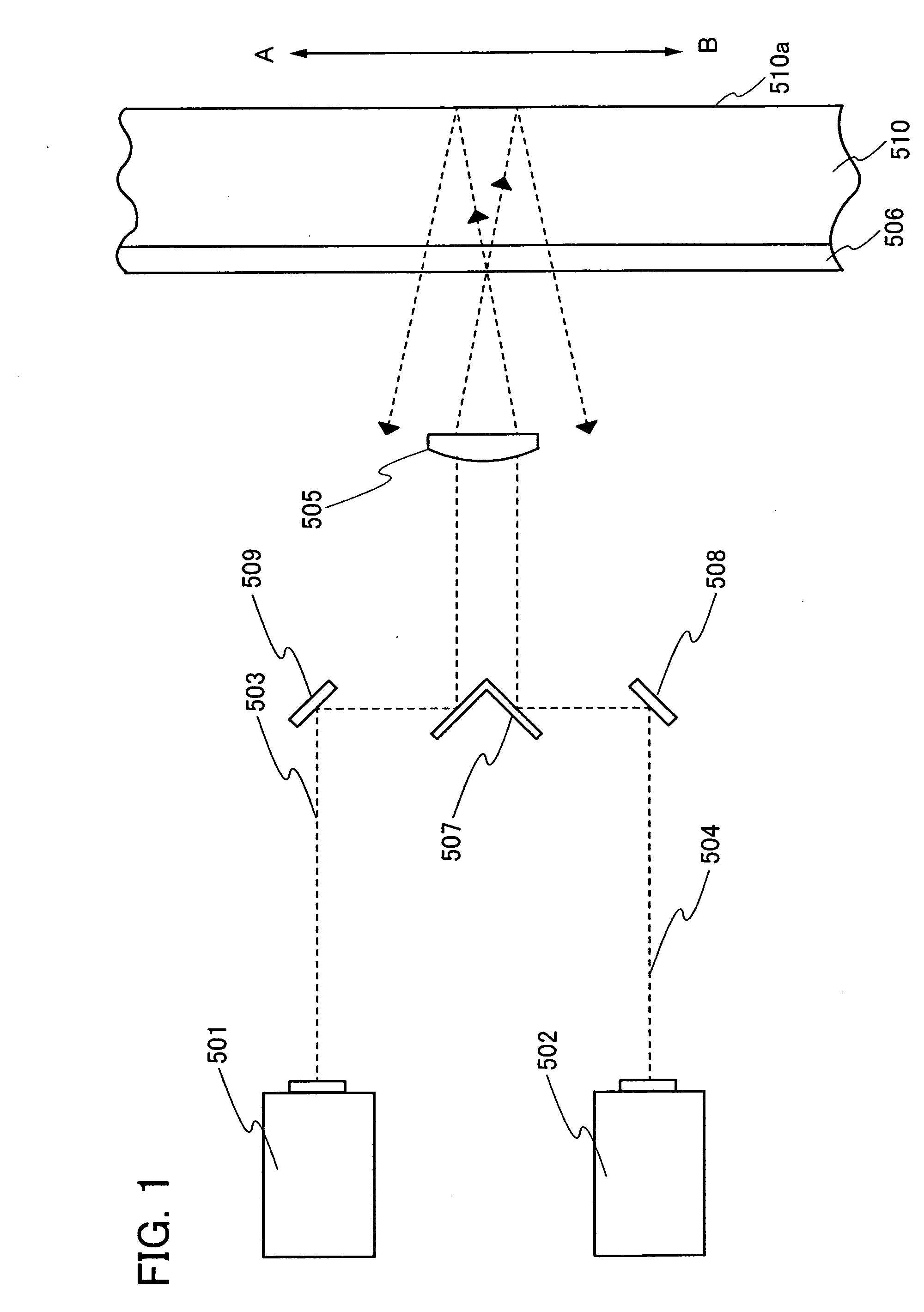
[0074]FIG. 1 is a diagram used to explain a crystallization method of a semiconductor film related to Embodiment Mode 1 of the present invention. This embodiment mode is a method in which a semiconductor film 506 is melted and crystallized through use of a laser irradiation apparatus. The semiconductor film 506 is formed over a substrate 510. The laser irradiation apparatus moves the substrate 510 back and forth in a direction along A-B in the diagram so that the position of irradiation by the laser beam relative to the semiconductor film 506 is moved.

[0075]The semiconductor film 506 is, for example, an amorphous or microcrystalline semiconductor film (an amorphous silicon film or a polysilicon film, for example). The substrate 510 is, for example, a glass substrate, a quartz substrate, a substrate formed of an insulator such as alumina, a plastic substrate with enough heat resistance to withstand post-process processing temperatures, a silicon substrate, or a metal plate. Furthermo...

embodiment mode 2

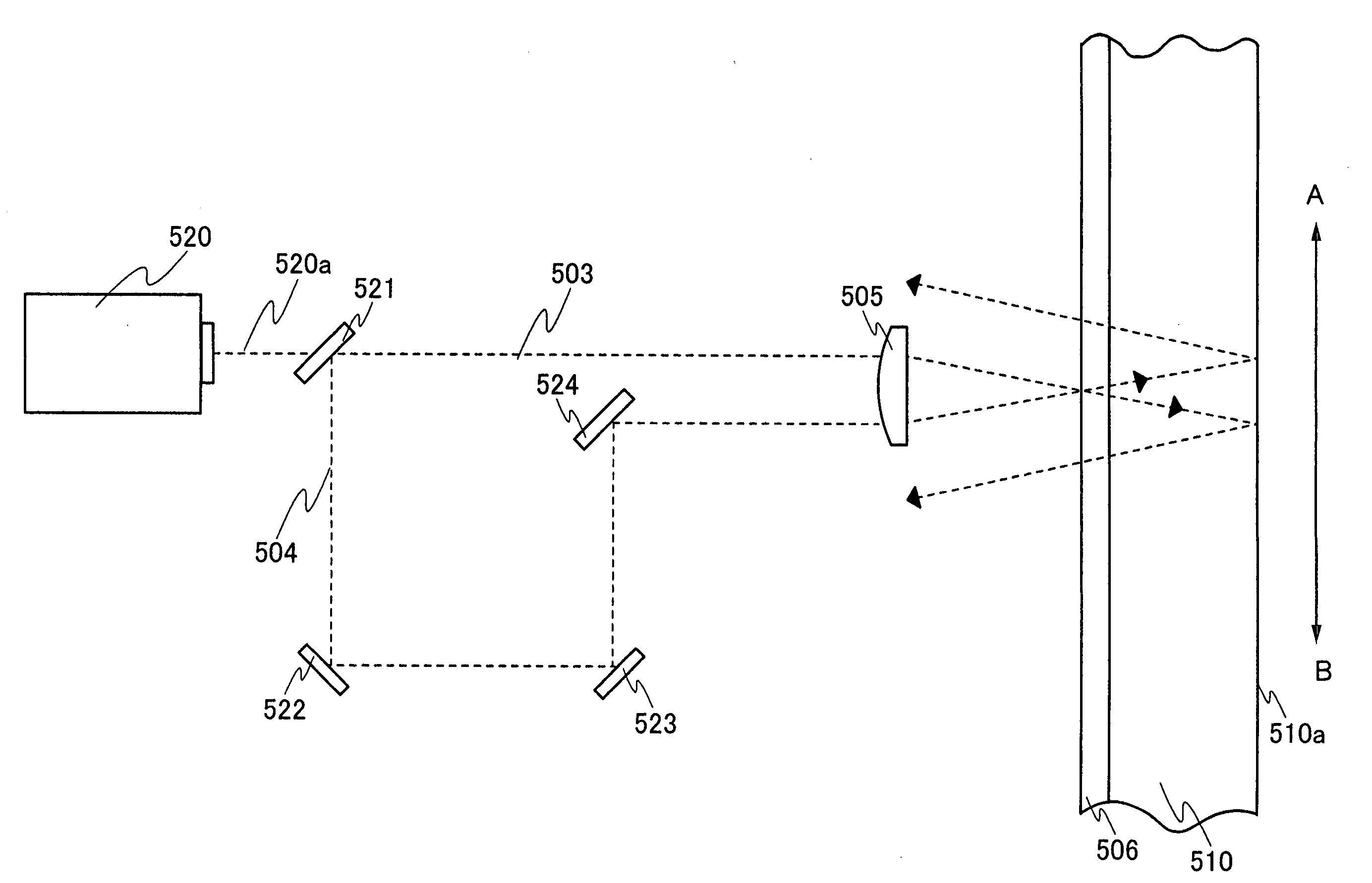
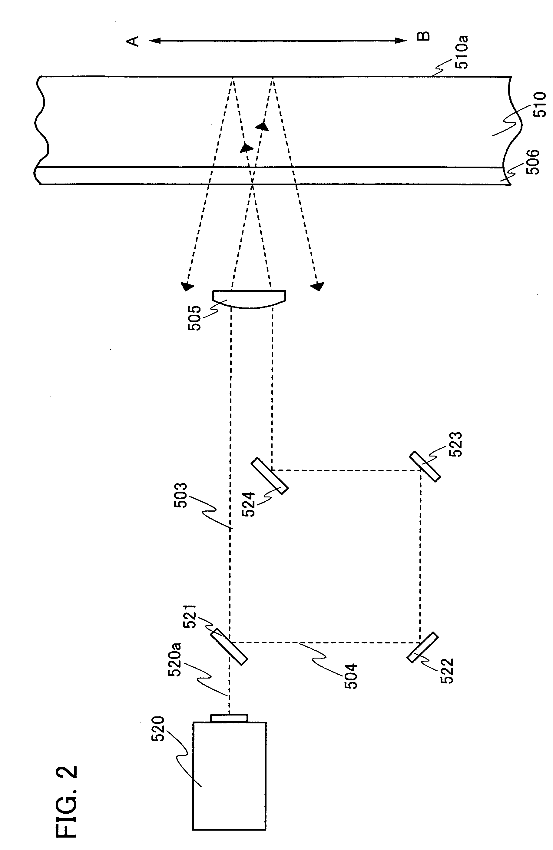
[0091]FIG. 2 is a diagram used to explain a crystallization method of a semiconductor film related to Embodiment Mode 2 of the present invention. The present Embodiment Mode 2 is the same as Embodiment Mode 1 except for the point that the laser irradiation apparatus has one oscillator and the beam of a mode-locked laser 520a oscillated by this oscillator 520 is split into two beams by a beam-splitter 521, generating a first laser beam 503 and a second laser beam 504; and the optical system up to where the first laser beam 503 and the second laser beam 504 are incident on a cylindrical lens 505. Specific examples of the mode-locked laser beam 520a are the same as the examples of the mode-locked laser given in Embodiment Mode 1. Hereinafter, the structures that are the same as those in Embodiment Mode 1 are referred to by the same numerals, and so, any explanation of these structures will be omitted.

[0092]The lengths of the optical paths of the first laser beam 503 and the second lase...

embodiment 1

[0099]One mode of a manufacturing method for a semiconductor device and a light-emitting device using the semiconductor device of Embodiment 1 will be explained with reference to FIGS. 3A to 3D, 4A to 4D, 5A and 5B, 6A to 6C, 7A and 7B, 8A and 8B, 9A and 9B, 10A and 10B, 11A and 11B, 12, and 13A to 13C.

[0100]First, after an insulating layer 101a is formed over a substrate 100, an insulating layer 101b is formed so as to be layered over the insulating layer 101a. It is preferable that the insulating layer 101a be formed so that the dispersion of impurities from the substrate 100 can be prevented, and it is preferable that the insulating layer 101a be formed using, for example, silicon nitride, silicon nitride that includes oxygen, or the like. Furthermore, it is preferable that the insulating layer 101b be formed as a layer in which the stress difference generated between the layer and a semiconductor film formed during a later step is decreased, and it is preferable that the insulat...


PUM

PropertyMeasurementUnit
oscillating frequencyaaaaaaaaaa
optical pathaaaaaaaaaa
temperatureaaaaaaaaaa

Abstract

A semiconductor film formed over a substrate is irradiated by a first laser beam which is incident on a bottom surface of the substrate at an angle and by a second laser beam which is incident on the bottom surface of the substrate at an angle opposite that of the first laser beam and oscillated by an oscillator differing from that of the first laser beam; whereby, part of the semiconductor film is melted, and a portion of the semiconductor film being melted is moved while the positions of irradiation of the first and the second laser beams and are being scanned approximately along the direction of slant for the first laser beam or the second laser beam.

Description

BACKGROUND OF THE INVENTION[0001]1. Field of the Invention[0002]The present invention relates to a semiconductor film crystallization method, a manufacturing method for a semiconductor device, and a laser irradiation apparatus. More specifically, the invention relates to a semiconductor film crystallization method, manufacturing method for a semiconductor device, and laser irradiation apparatus in which the generation of in-plane variations in the quality of a semiconductor film which has been crystallized can be suppressed.[0003]2. Description of the Related Art[0004]In recent years, extensive research has been conducted on laser crystallization methods used to crystallize a semiconductor film (for example, an amorphous semiconductor film) formed over a glass substrate through irradiation of the semiconductor film with a laser beam.[0005]Crystallization of a semiconductor film is performed in order to increase carrier mobility through crystallization of the semiconductor film. The ...

Claims


Application Information

Patent Timeline
Patent Type & Authority Applications(United States)
IPC IPC(8): H01L21/84
CPCB23K26/0613B23K26/0676B23K26/0738H01L21/0237H01L21/02532H01L27/1285H01L21/02678H01L21/02691H01L27/1266H01L27/1255H01L21/02672
Inventor TANAKA, KOICHIRO
Owner SEMICON ENERGY LAB CO LTD
Why Eureka
Try Eureka