Electron microscope and electron bean inspection system.

a technology of electron bean and electron microscope, which is applied in the direction of material analysis using wave/particle radiation, instruments, nuclear engineering, etc., can solve the problems of low rate of secondary electron usable for image forming, the microscope projector that uses secondary electrons and mirror electrons suffers, and the rate of secondary electrons is not always available for image forming, etc., to avoid degradation of image resolution, high energy part, and high resolution image

Inactive Publication Date: 2007-08-09
HITACHI HIGH-TECH CORP
View PDF6 Cites 30 Cited by
  • Summary
  • Abstract
  • Description
  • Claims
  • Application Information

AI Technical Summary

Benefits of technology

[0008]There is another system that magnifies and projects mirror electrons reflected without colliding with the object specimen just before it instead of using secondary electrons and back-scattered electrons. The system is referred to as a mirror electron microscope. This mirror electron microscope can be used to detect disturbed potentials and shapes caused by defects, thereby detecting defects. If an object pattern has any protruded part or is negatively charged, the equipotential plane formed on the specimen functions like a convex lens with respect to entered electrons. If the pattern has any recessed part or is more positively charged than the peripheral areas, the equipotential plane formed on the specimen functions like a concave lens. These convex or concave lenses on the specimen cause the mirror electrons to slightly change their trajectories. To cope with this, the focal condition of the imaging lens is adjusted, in order to use most of those mirror electrons for image forming. In other words, using mirror electrons such way makes it possible to obtain images with a high S / N ratio and to reduce the inspection time.
[0010]Under such circumstances, it is an object of the present invention to solve the above-described conventional problems to obtain stable mirror electron images and provide a defect inspection system capable of detecting defects of a pattern formed on a wafer quickly and very accurately.
[0012]The first method of the present invention inheres means provided for controlling a reflecting plane that reflects mirror electrons. Concretely, if 0V is assumed as a voltage applied to an electron source and Vs is assumed as a voltage applied to a specimen, an entered electron beam is reflected without colliding with the specimen when Vs<V0 is satisfied, that is, when Vs reaches a negative potential under V0. Such a condition is referred to as a mirror reflection condition. However, the means of the present invention provided for controlling this potential difference V0−Vs can optimize the contrast of mirror electron images.
[0015]As described above, if means for controlling the reflecting plane of an illuminating electron beam to be assumed as a mirror electron beam is provided according to the type and state of the object specimen, pattern sizes and charged levels can be distinguished, thereby observation and inspection are made more quickly and accurately.
[0017]It is also possible to avoid degradation of the image resolution to be caused by charging of the specimen by eliminating only the high energy part of the electron beam. If an electron beam is illuminated onto an insulation specimen having less current leaks, the specimen surface potential rises up to a negative potential at which no electron comes to collide with the specimen. In other words, as shown in FIG. 6A, if the high energy part of an illuminating electron beam has a tail, the specimen potential rises from the potential Vs (FIG. 6B) at the initial time of illumination up to a potential (FIG. 6C) at which the highest energy part electrons in the tail do not collide with the specimen, thereby the illuminating beam goes away from the specimen. In such a case, it is difficult to obtain fine information of the specimen surface, thereby the image becomes unclear. This is why an energy filter is used in such a case to eliminate only the high energy part of the electron beam. A high resolution image is thus obtained (FIG. 6D) while the illuminating beam does not go away from the specimen.
[0018]Furthermore, only the low energy part of the electron beam is eliminated to eliminate the information obtained from the long cycle structure away from the specimen.

Problems solved by technology

However, the projection type microscope that uses secondary electrons and mirror electrons suffers from the following problems.
At this time, all the emitted secondary electrons are not always available for forming an image.
Such way, because the rate of the secondary electrons usable for image forming actually is low, it is difficult to secure a proper S / N ratio of images even when using the secondary electrons obtained by illuminating a large current onto a specimen with an area electron beam to form images at a time.
Thus the inspection time cannot be reduced as expected.
Thus it is difficult to achieve a good balance between high resolution and high speed like the case using secondary electrons.

Method used


Image

  • Electron microscope and electron bean inspection system.
  • Electron microscope and electron bean inspection system.
  • Electron microscope and electron bean inspection system.

Examples


first embodiment

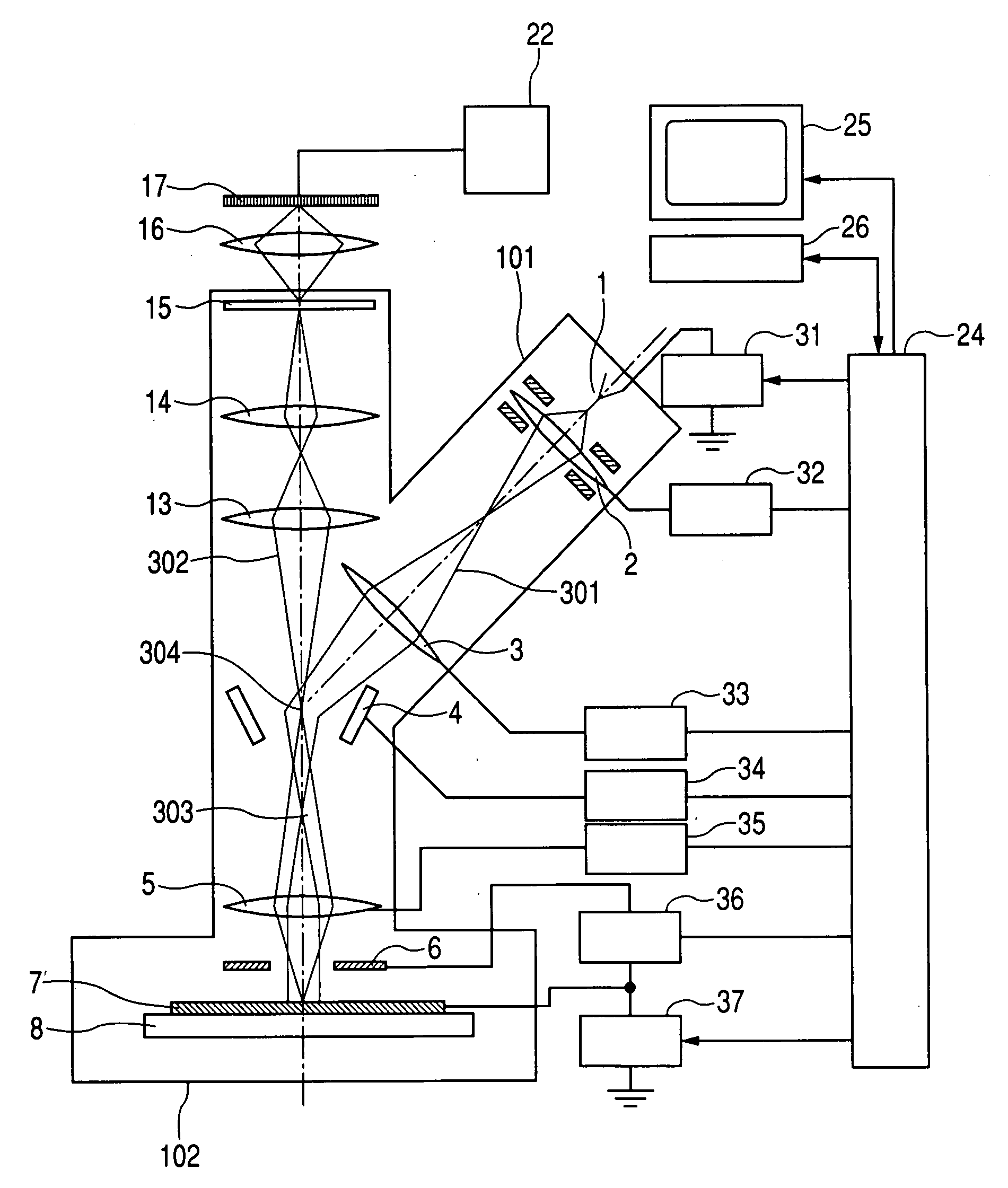
[0048]FIG. 1 shows a configuration of a mirror electron beam microscope for describing the operation in the first embodiment. An ExB deflector 4 used as a beam separator is disposed nearly to an imaging plane of a reflecting electron beam 302 that includes a mirror electron beam. An illumination system optical axis and an imaging system optical axis perpendicular to a wafer 7 respectively cross each other at a θIN angle. As described above, because an ExB deflector 4 used as a beam separator is disposed between a condenser 3 and an objective lens 5, the illuminating electron beam 301 emitted from an electron source 1 is deflected by the ExB deflector 4 to an optical axis perpendicular to the wafer 7. Electrons of the illuminating electron beam 301 deflected by the ExB deflector 4 are focused by the condenser lens 3 in the vicinity of a focal plane 303 of the objective lens 5, thereby the electrons of the illuminating electron beam 301 are illuminated onto the specimen 7 almost in pa...

second embodiment

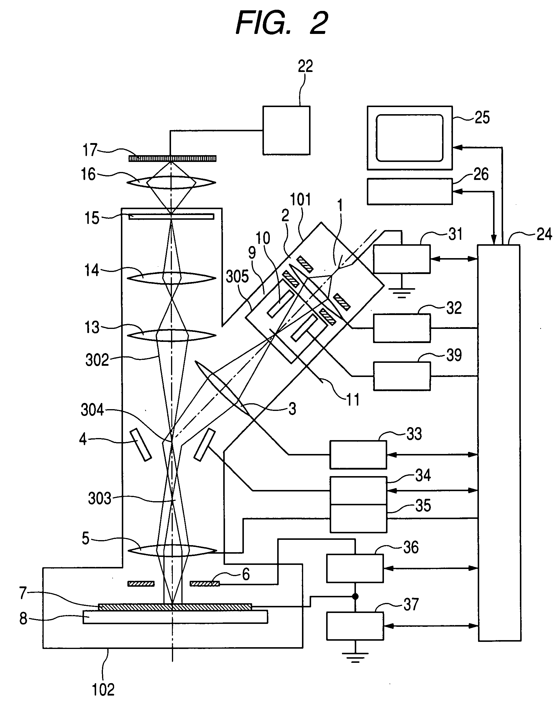
[0063]In this second embodiment shown in FIG. 2, an energy filter is mounted in an illuminating system of a mirror electron microscope to control the mirror reflecting plane. An energy filter 9 is disposed between an electron gun lens 2 and a condenser lens 3. An illuminating electron beam 101 emitted from an electron source 1 and passed through the energy filter 9 forms an energy-dispersed cross-over between the energy filter 9 and the condenser lens 3. On the cross-over is disposed a limiting stop 11 for selecting an energy of the illuminating electron beam. The illuminating electron beam 101 of which energy is selected is deflected to an optical axis perpendicular to a wafer 7 by a beam separator 4 disposed between the condenser lens 3 and an objective lens 5, then focused in the vicinity of an objective lens focal plane 303 by the condenser lens 3. The electrons of the illuminating electron beam can thus be illuminated perpendicularly onto a specimen 7 almost in parallel. The li...

third embodiment

[0072]In this third embodiment shown in FIG. 3, a mirror electron microscope is employed for quick wafer inspection. An electron source 1 is a Zr / 0 / W type Schottky electron source having a tip of which radius is about 1 μm. With the use of this electron source, a uniform planar electron beam can be formed stably with a large current (ex., 1.5μ A) and at an energy width of 0.5 eV or under.

[0073]An energy filter 9 is disposed between an electron gun lens 2 and a condenser lens 3 and an illuminating electron beam 301 emitted from the electron source 1 passes through the energy filter 9, then forms an energy dispersed cross-over between the energy filter 9 and the condenser lens 3. On the cross-over is disposed a limiting stop 11 used to select an energy of the illuminating electron beam 101. The illuminating electron beam 101 of which an energy is selected passes the condenser lens 3, then deflected to an optical axis perpendicular to a wafer 7 by a beam separator disposed between the ...


PUM


Abstract

While an image obtained by a general electron microscope is affected by the shape and material of an object specimen, an image obtained from mirror electrons is affected by the shape of an equipotential surface on which the mirror electrons are reflected, thereby the image interpretation is complicated. A mirror electron microscope of the present invention is provided with the following means for controlling a reflecting plane of the mirror electrons according to the structure of an object pattern to be measured or a concerned defect.1) Means for controlling a potential difference between a specimen and an electron source equivalent to a height of a reflecting plane of a mirror electron beam according to a type, an operation condition of an electron source, and a type of a pattern on a specimen.2) Means for controlling an energy distribution of an illuminating beam with an energy filter 9 disposed in an illuminating system.It is thus possible to inspect a specimen according to a size and a potential of a pattern, which are distinguished from others.

Description

CLAIM OF PRIORITY[0001]The present application claims priority from Japanese application JP 2006-027850 filed on Feb. 6, 2006, the content of which is hereby incorporated by reference into this application.FIELD OF THE INVENTION[0002]The present invention relates to a reflection electron microscope such as a mirror electron microscope for observing a state of a surface of a specimen (semiconductor specimen, or the like) or a defect inspection system for inspecting a pattern defect, a foreign matter, etc. on a semiconductor wafer using the reflection electron microscope.BACKGROUND OF THE INVENTION[0003]There is a detecting method for circuit pattern defects on a wafer by comparing images in a manufacturing process of a semiconductor device. According to the method, an electron beam is illuminated onto a specimen to detect fine etching residuals under the resolving power of the optical microscope, such shape defects as fine pattern defects, as well as such electrical defects as non-ap...

Claims


Application Information

Patent Timeline
Patent Type & Authority Applications(United States)
IPC IPC(8): G21K7/00
CPCH01J37/29H01J2237/057H01J2237/2817H01J2237/24592H01J2237/2538H01J2237/1508
Inventor MURAKOSHI, HISAYATODOKORO, HIDEOSHINADA, HIROYUKIHASEGAWA, MASAKIENYAMA, MOMOYO
Owner HITACHI HIGH-TECH CORP
Why Eureka
Try Eureka