

Silicon electrode plate for plasma etching with superior durability
a technology of plasma etching and silicon electrode plate, which is applied in the direction of plasma technique, electric discharge tube, semiconductor device, etc., can solve the problems of wasteful mode of use, irregular etching of wafers, and the inability to avoid the above-described abrasion holes b>3, so as to reduce the frequency of replacement of silicon electrode plate for plasma etching due to plasma etching.
- Summary
- Abstract
- Description
- Claims
- Application Information
AI Technical Summary
Benefits of technology
Problems solved by technology
Method used
Image

Examples
embodiment 1
[0028] Si raw material with a purity of 11 N was melted, and initially doped with B and P so as to prepare a Si melt containing 1 to 15 ppba of B and 1 to 10 ppba of P. Using this Si melt, a silicon single crystal having a diameter of 300 mm was prepared by the CZ method. After circular cutting and slicing this ingot at a thickness of 8 mm by a diamond band saw, a silicon single crystal electrode substrate with a diameter of 290 mm and a thickness of 6 mm was prepared by grinding.
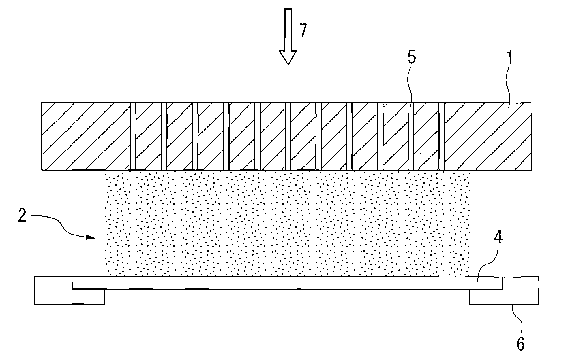
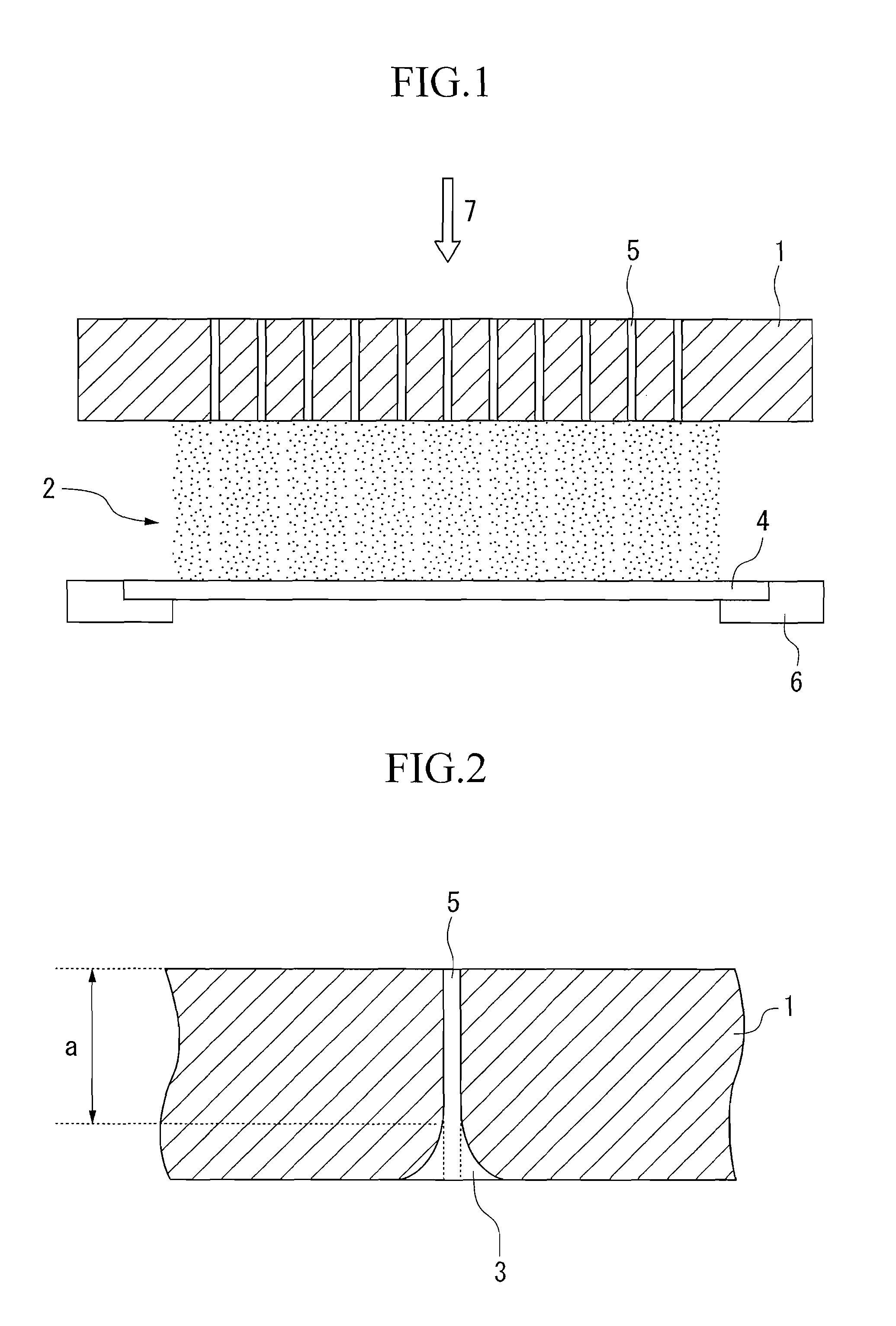
[0029] Etching gas ejecting through-holes with a diameter of 0.3 mm were formed at 5 mm intervals in this silicon single crystal electrode substrate, and then this silicon single crystal electrode substrate was immersed in a liquid mixture of hydrofluoric acid, acetic acid and nitric acid for 5 minutes so as to remove the surface machining layer; whereby were prepared silicon electrode plates for plasma etching of the present invention (hereinafter, electrode plates of the present invention) 1 to 14 contai...
embodiment 2
[0039] Si raw material with a purity of 11 N was melted, and initially doped with B and As so as to prepare a Si melt containing 1 to 15 ppba of B and 1 to 10 ppba of As. Using this Si melt, silicon single crystal silicon having a diameter of 300 mm was prepared by the CZ method. After circular cutting and slicing this ingot at a thickness of 8 mm by a diamond band saw, a silicon single crystal electrode substrates with a diameter of 290 mm and a thickness of 6 mm was prepared by grinding.
[0040] Etching gas ejecting through-holes with a diameter of 0.3 mm were formed at 5 mm intervals in this silicon single crystal electrode substrate, and then this silicon single crystal electrode substrate was immersed in a liquid mixture of hydrofluoric acid, acetic acid and nitric acid for 5 minutes so as to remove the surface machining layer; whereby 5 were prepared electrode plates of the present invention 15 to 28, comparative silicon electrode plates 3 and 4, and conventional electrode plat...
embodiment 3
[0050] Si raw material with a purity of 11 N was melted, and initially doped with B, P and As so as to prepare a Si melt containing 1 to 15 ppba of B and 1 to 10 ppba of P+As. Using this Si melt, silicon single crystal having a diameter of 300 mm was prepared by the CZ method. After circular cutting and slicing this ingot at a thickness of 8 mm by a diamond band saw, a silicon single crystal electrode substrates with a diameter of 290 mm and a thickness of 6 mm was prepared by grinding.
[0051] Etching gas ejecting through-holes with a diameter of 0.3 mm were formed at 5 mm intervals in this silicon single crystal electrode substrate, and then this silicon single crystal electrode substrate was immersed in a liquid mixture of hydrofluoric acid, acetic acid and nitric acid for 5 minutes so as to remove the surface machining layer; whereby were prepared electrode plates of the present invention 29 to 33, and comparative silicon electrode plates 5 and 6.
[0052] The B, P and As contents ...
PUM
| Property | Measurement | Unit |
|---|---|---|
| diameter | aaaaa | aaaaa |
| thickness | aaaaa | aaaaa |
| diameter | aaaaa | aaaaa |
Abstract
Description
Claims
Application Information