Crystal substrates and methods of fabricating the same

a technology of crystal substrates and substrates, which is applied in the direction of crystal growth process, polycrystalline material growth, spades, etc., can solve the problems of limited size reduction of related art semiconductor devices, relative high fabricating costs of related art methods of fabricating single layer soi substrates, and may reach a performance breaking point. , to achieve the effect of easy controllable thickness

Inactive Publication Date: 2007-08-16
SAMSUNG ELECTRONICS CO LTD
View PDF31 Cites 87 Cited by
  • Summary
  • Abstract
  • Description
  • Claims
  • Application Information

AI Technical Summary

Benefits of technology

[0009]Example embodiments related to single crystal substrates and methods of fabricating the same. For example, example embodiments provide a single crystal silicon substrate and a s...

Problems solved by technology

Size reduction of related art semiconductor devices may be limited because of a performance limitation on wafer-type single crystal silicon.
For example, wafer-type single crystal silicon used in related art semiconductor devices may reach a performance breaking point due to compactness of transistors.
However, related art methods of fabricating single layer SOI substrates may have relative high fabricating costs.
In addition, if single layer SOI substrates are stacked in several layers, the fabricating cost may increase.
Furthermore, elements fabricated on a lower layer may break while fabricating an upper layer (e.g., a single crystal stacked layer).
In addition, the substrate formed may experience a thermal impact while enduring the higher temperature process.
As ...

Method used


Image

  • Crystal substrates and methods of fabricating the same
  • Crystal substrates and methods of fabricating the same
  • Crystal substrates and methods of fabricating the same

Examples


Embodiment Construction

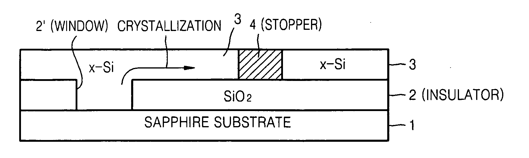
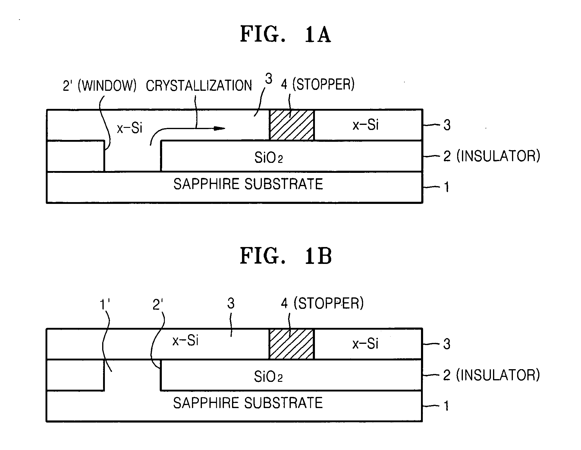
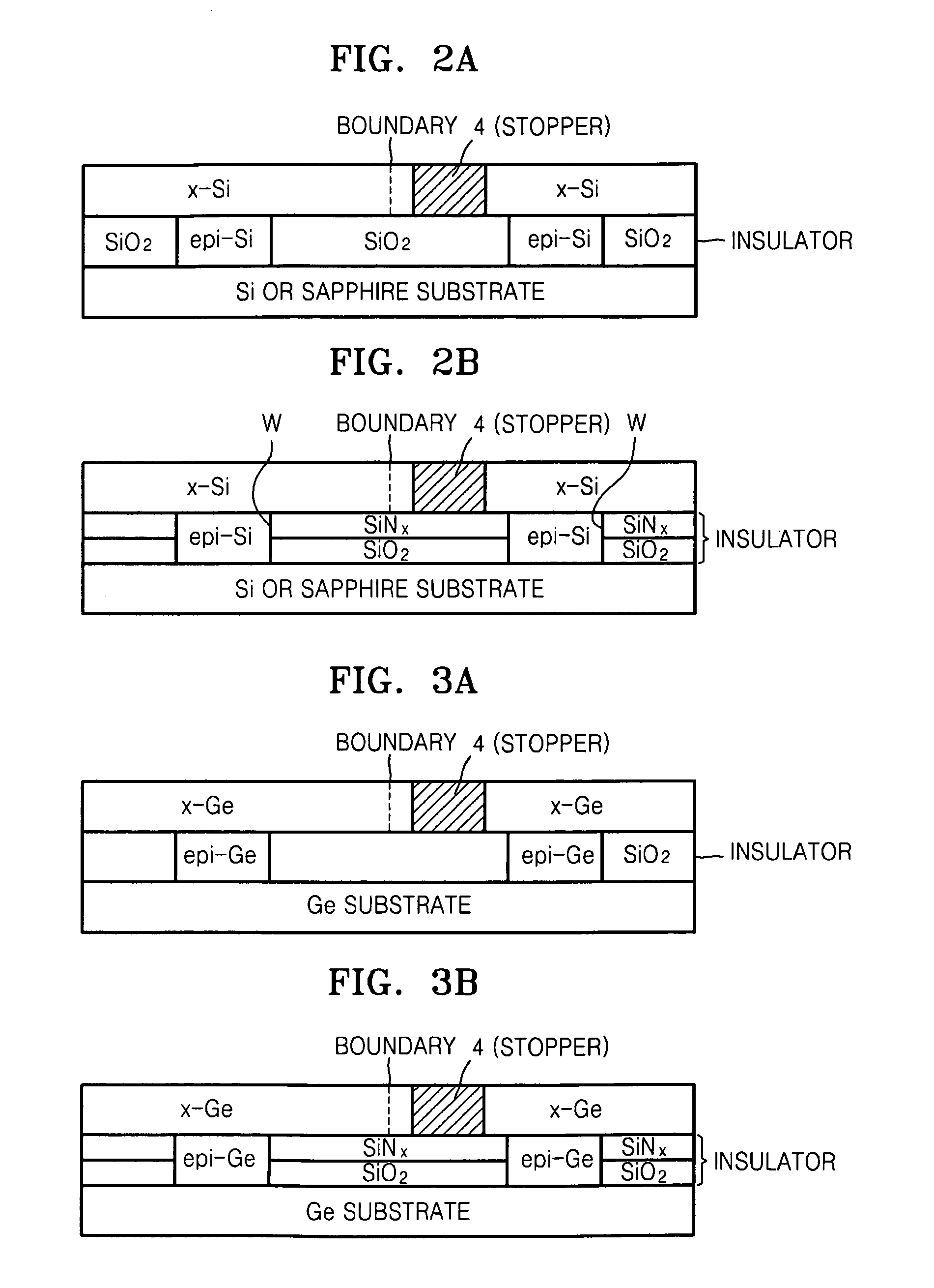
[0021]Various example embodiments will now be described more fully with reference to the accompanying drawings in which some example embodiments are shown. In the drawings, the thicknesses of layers and regions are exaggerated for clarity.

[0022]Detailed illustrative example embodiments are disclosed herein. However, specific structural and functional details disclosed herein are merely representative for purposes of describing example embodiments. This invention may, however, may be embodied in many alternate forms and should not be construed as limited to only the example embodiments set forth herein.

[0023]Accordingly, while example embodiments are capable of various modifications and alternative forms, embodiments thereof are shown by way of example in the drawings and will herein be described in detail. It should be understood, however, that there is no intent to limit example embodiments to the particular forms disclosed, but on the contrary, example embodiments are to cover all...


PUM


Abstract

A single crystal substrate and method of fabricating the same are provided. The single crystal substrate includes an insulator having a window exposing a portion of a substrate, a selective epitaxial growth layer formed on the portion of the substrate exposed through the window and a single crystalline layer formed on the insulator and the selective epitaxial growth layer using the selective epitaxial growth layer as an epitaxial seed layer.

Description

PRIORITY STATEMENT[0001]This non-provisional U.S. patent application claims priority under 35 U.S.C. §119 to Korean Patent Application No. 10-2006-0015151, filed on Feb. 16, 2006, in the Korean Intellectual Property Office (KIPO), the entire contents of which is incorporated herein by reference.BACKGROUNDDescription of the Related Art[0002]Size reduction of related art semiconductor devices may be limited because of a performance limitation on wafer-type single crystal silicon. For example, wafer-type single crystal silicon used in related art semiconductor devices may reach a performance breaking point due to compactness of transistors. In the related art, silicon on insulators (SOIs) have been used to attempt to suppress this limitation. SOIs are formed by depositing single crystal silicon on insulators to improve the performance of the elements without reducing the dimensions of the elements.[0003]SOIs are single crystal silicon substrates that are parasitic, have a high mobility...

Claims


Application Information

Patent Timeline
IPC IPC(8): H01L31/00C30B13/02C30B19/00H01L29/04
CPCC30B23/025C30B25/18H01L21/02381H01L21/0242H01L21/30625H01L21/02532H01L21/02538H01L21/02639H01L21/02675H01L21/02521A01C15/122A01C15/006A01B49/06
Inventor NOGUCHI, TAKASHICHO, HANS S.XIANYU, WENXUYIN, HUAXIANG
Owner SAMSUNG ELECTRONICS CO LTD
Why Eureka
Try Eureka