Ultra-thin logic and backgated ultra-thin SRAM

Inactive Publication Date: 2007-08-16
IBM CORP
View PDF6 Cites 28 Cited by
  • Summary
  • Abstract
  • Description
  • Claims
  • Application Information

AI Technical Summary

Benefits of technology

[0007] In view of the foregoing, an embodiment of the invention provides a semiconductor structure that comprises both a first device (e.g., a static random access memory (SRAM) cell) that incorporates FETs configured for precise threshold voltage (Vt) control and a second device (e.g., a logic circuit) that incorporates FETs configured to have

Problems solved by technology

However, instead of a back gate for each second FET, a second portion of the semiconductor layer below the second device remains un-doped (i.e., intrinsic).
Despite the resultant performance degradation due to parasitic back gate capacitance, these back gates result in a net gain for devices such a

Method used


Image

  • Ultra-thin logic and backgated ultra-thin SRAM
  • Ultra-thin logic and backgated ultra-thin SRAM
  • Ultra-thin logic and backgated ultra-thin SRAM

Examples


Embodiment Construction

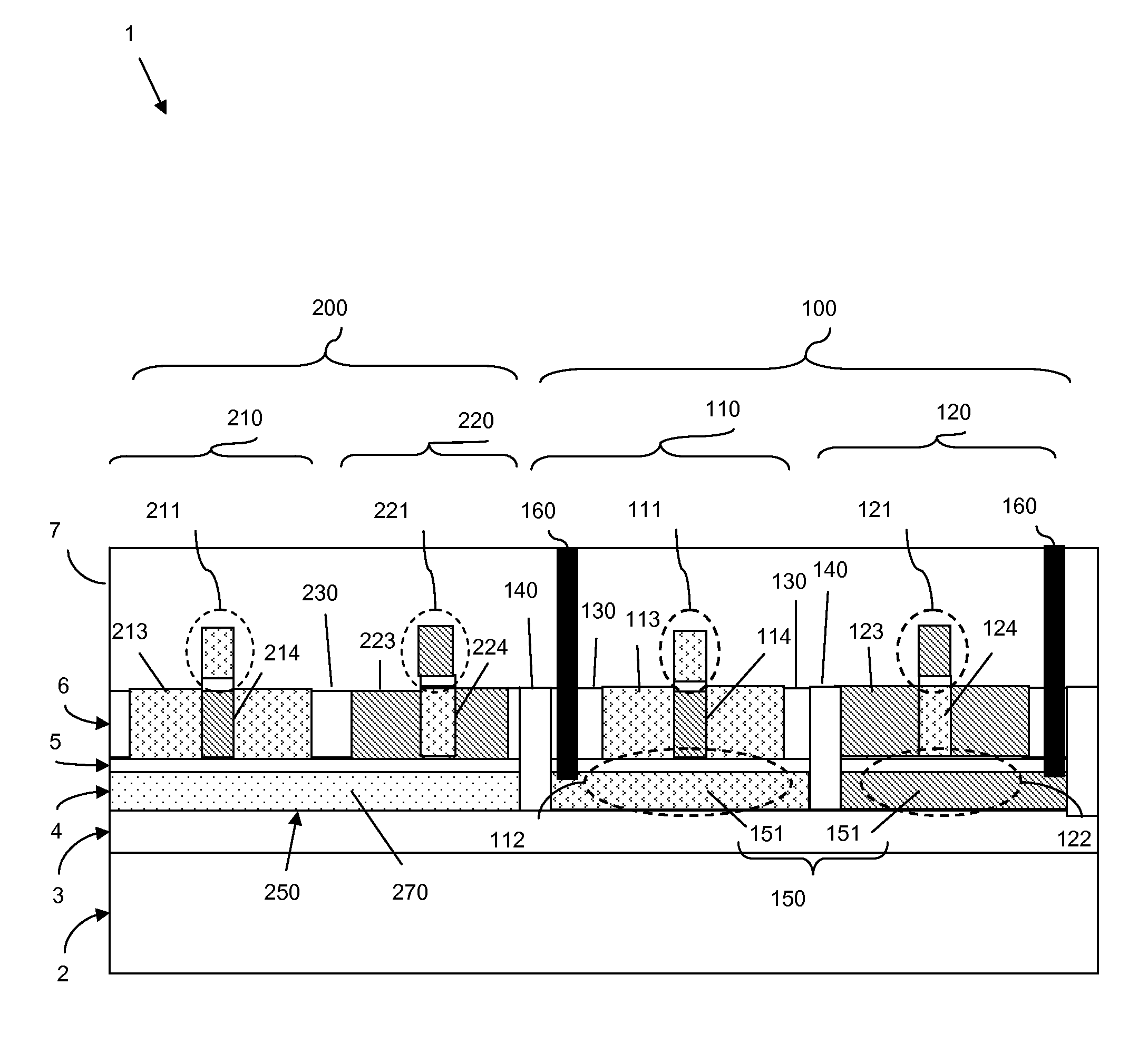
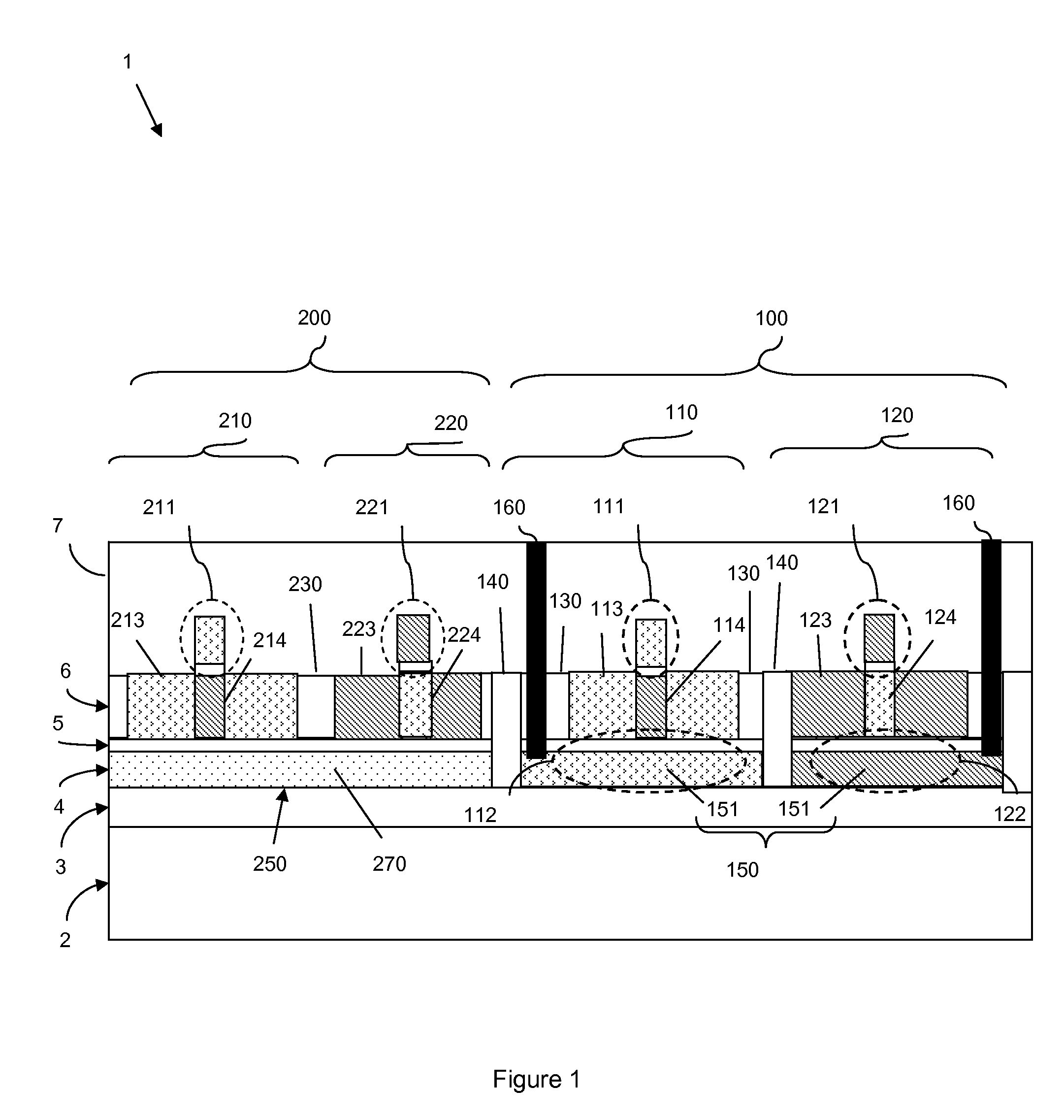
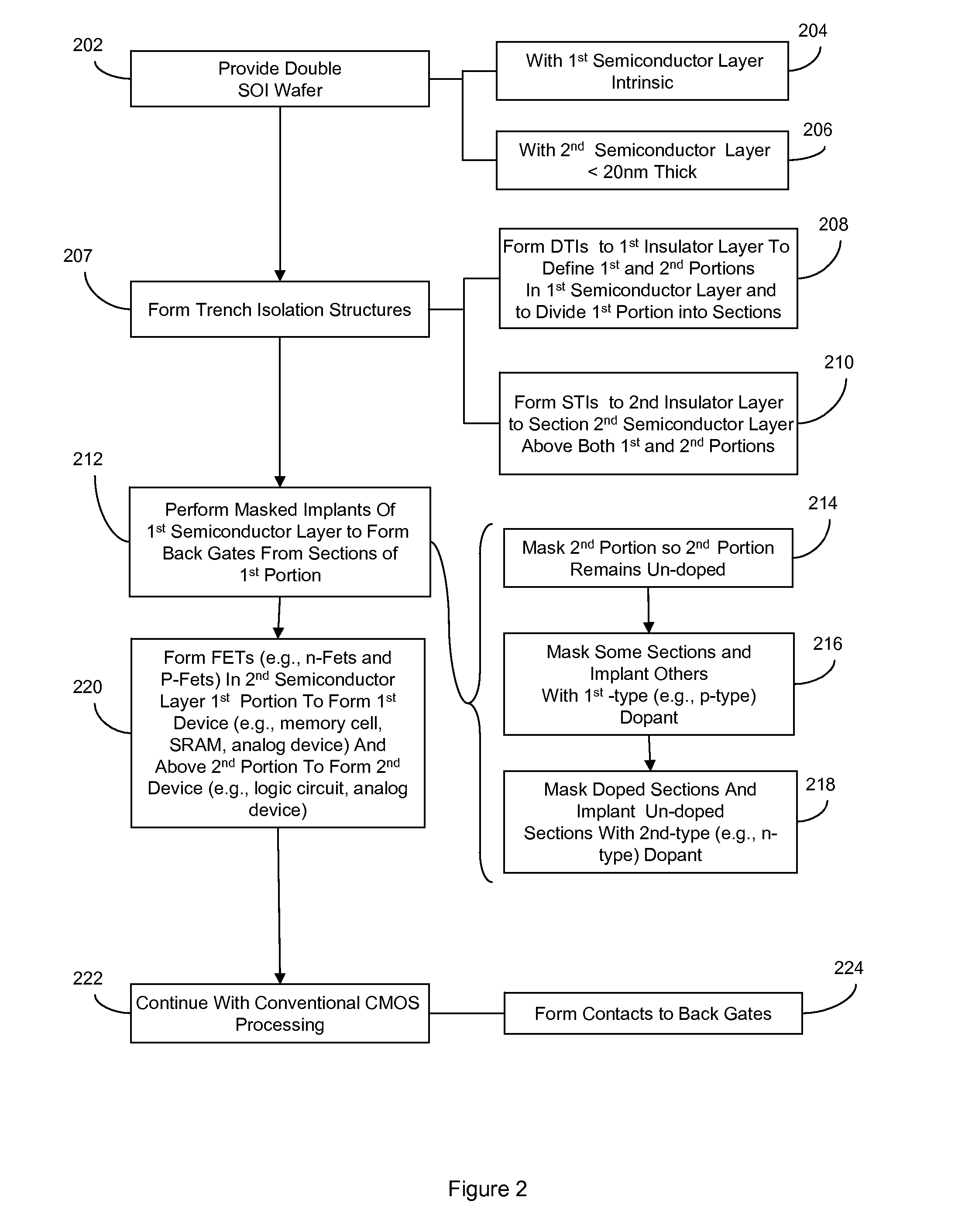
[0031] The embodiments of the invention and the various features and advantageous details thereof are explained more fully with reference to the non-limiting embodiments that are illustrated in the accompanying drawings and detailed in the following description. It should be noted that the features illustrated in the drawings are not necessarily drawn to scale. Descriptions of well-known components and processing techniques are omitted so as to not unnecessarily obscure the embodiments of the invention. The examples used herein are intended merely to facilitate an understanding of ways in which the embodiments of the invention may be practiced and to further enable those of skill in the art to practice the embodiments of the invention. Accordingly, the examples should not be construed as limiting the scope of the embodiments of the invention.

[0032] As mentioned above, semiconductor devices that do not need fast switching speeds but require precise Vt control (e.g., static random ac...


PUM


Abstract

Disclosed are embodiments of a structure that comprises a first device, having multiple FETs, and a second device, having at least one FET. Sections of a first portion of a semiconductor layer below the first device are doped and contacted to form back gates. A second portion of the semiconductor layer below the second device remains un-doped and un-contacted and, thus, functions as an insulator. Despite the performance degradation of the first device due to back gate capacitance, the back gates result in a net gain for devices such as, SRAM cells, which require precise Vt control. Contrarily, despite marginal Vt control in the second device due to the absence of back gates, the lack of capacitance loading and the added insulation result in a net gain for high performance devices such as, logic circuits.

Description

BACKGROUND [0001] 1. Field of the Invention [0002] The embodiments of the invention generally relate ultra thin semiconductor devices and, more particularly, to a semiconductor structure and method of forming the structure that incorporates a first ultra-thin device having field effect transistors (FETs) with both front and back gates and a second ultra-thin device having FETs with only front gates. [0003] 2. Description of the Related Art [0004] Ultra-thin silicon-on-insulator (UTSOI) field effect transistors (FETs) formed from wafers in which the active silicon layer is less 20 nm thick and therefore, fully depleted, show promise for incorporation into various semiconductor devices (e.g., logic circuits, memory cells, SRAM cells, analog devices, etc). [0005] Such FETs can be formed either with or without back gates and the decision to form them with or without the back gates involves a trade-off between the need for threshold voltage (Vt) control and the need to avoid device perfo...

Claims


Application Information

Patent Timeline
IPC IPC(8): H01L21/337H01L29/94
CPCH01L21/84H01L27/1203H01L27/11H10B10/00
Inventor ANDERSON, BRENT A.BRYANT, ANDRESCLARK, WILLIAM F. JR.NOWAK, EDWARD J.
Owner IBM CORP
Why Eureka
Try Eureka