Semiconductor photonic devices with enhanced responsivity and reduced stray light

Active Publication Date: 2007-08-16
INFRARED NEWCO
View PDF30 Cites 107 Cited by
  • Summary
  • Abstract
  • Description
  • Claims
  • Application Information

AI Technical Summary

Benefits of technology

[0007] In accordance with the invention, a photonic device comprises a semiconductor substrate including at least one circuit component comprising a metal silicide layer and an overlying layer including at least one photoresponsive component. The metal silicide layer is disposed between the circuit component and the photoresponsive component to prevent entry into the circuit component of light that penetrates the photoresponsive component. The silicide layer advantageously reflects the light back into the photoresponsive elemen

Problems solved by technology

Light transmitted through the photoresponsive component can penetrate into the substrate, where it becomes stray light that can be absorbed (directly or after reflection) in the semiconductor circuitry, causing unexpected and undesired current to flow.
Such stray light causes undesired

Method used


Image

  • Semiconductor photonic devices with enhanced responsivity and reduced stray light
  • Semiconductor photonic devices with enhanced responsivity and reduced stray light
  • Semiconductor photonic devices with enhanced responsivity and reduced stray light

Examples


Embodiment Construction

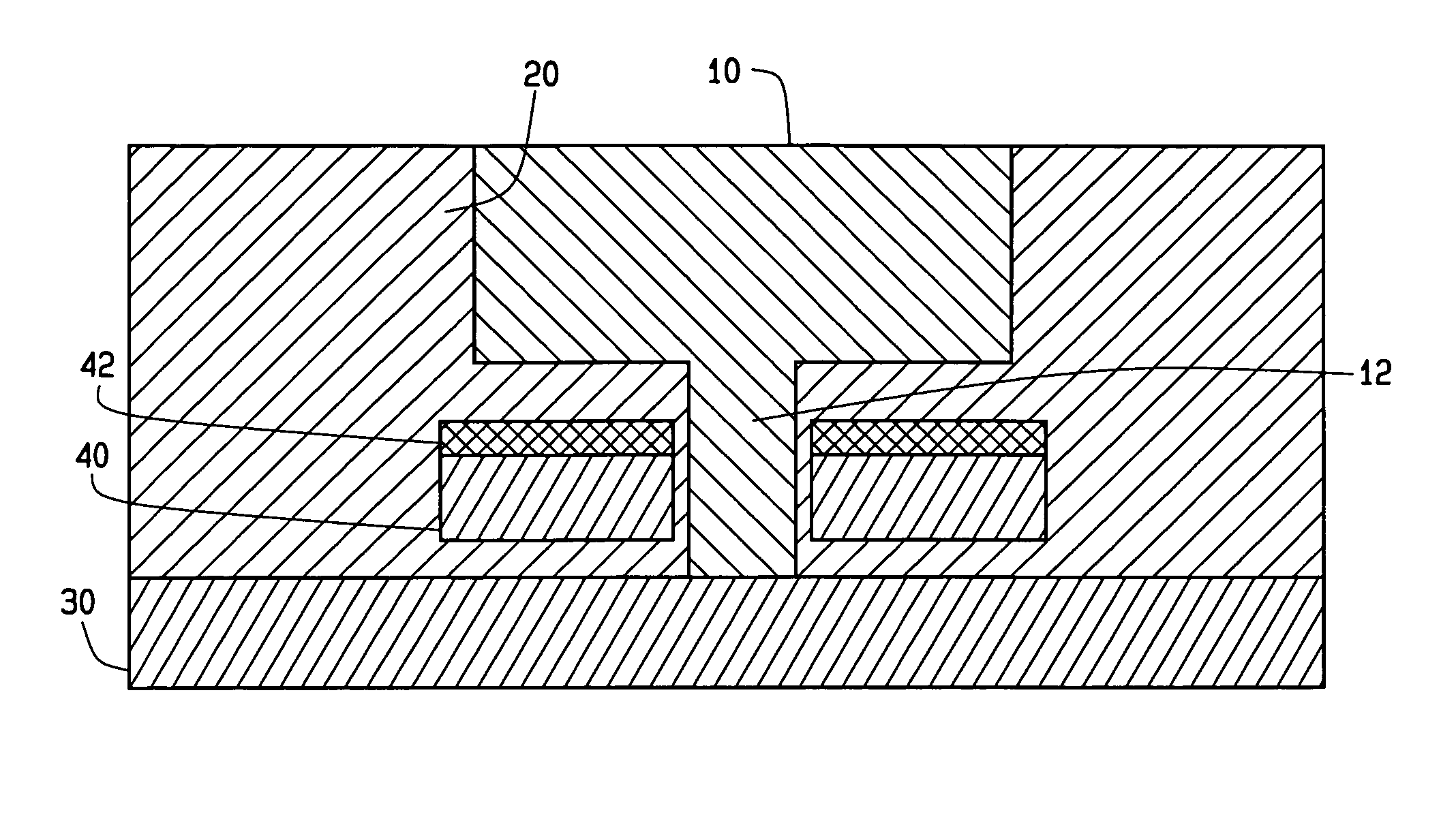
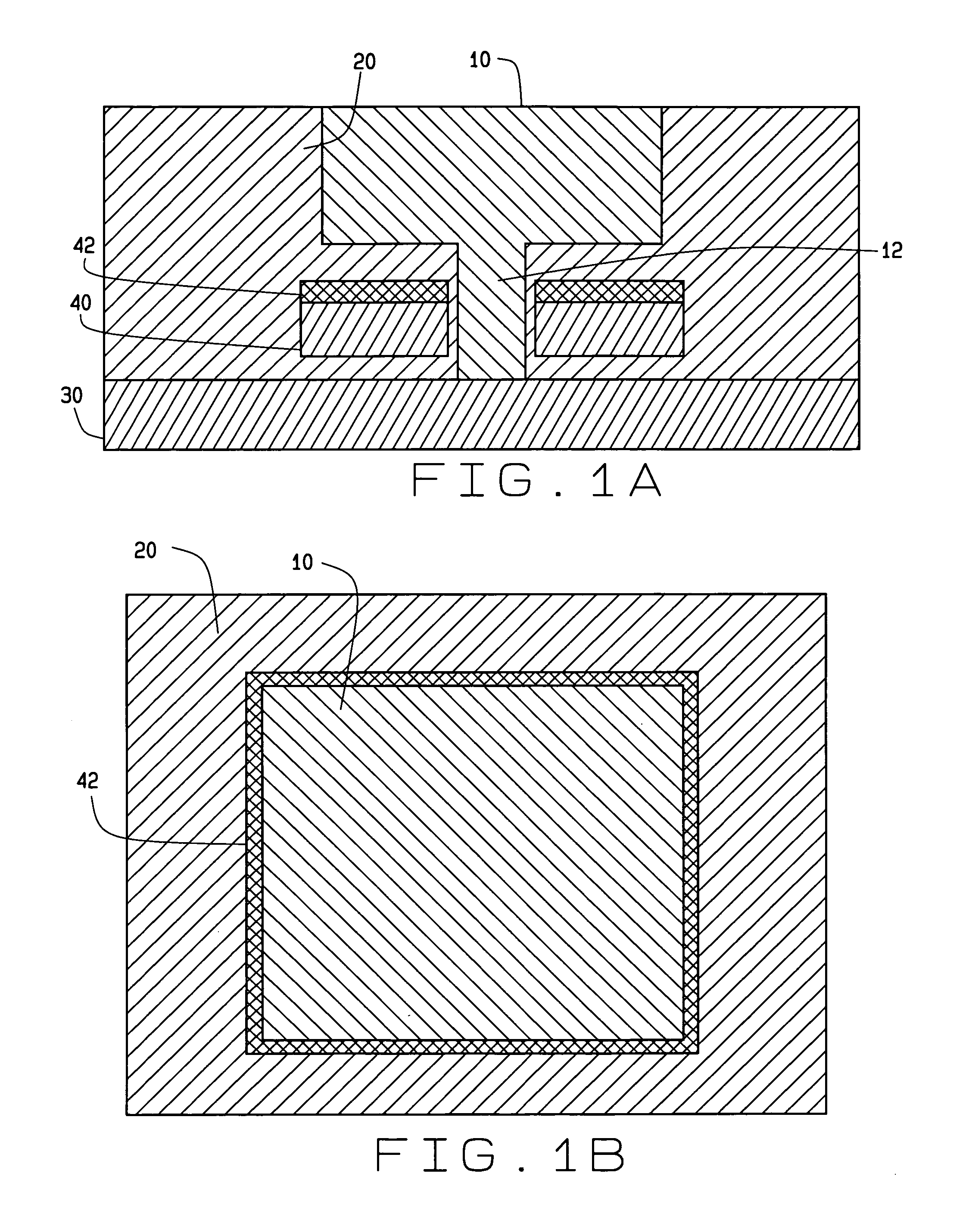
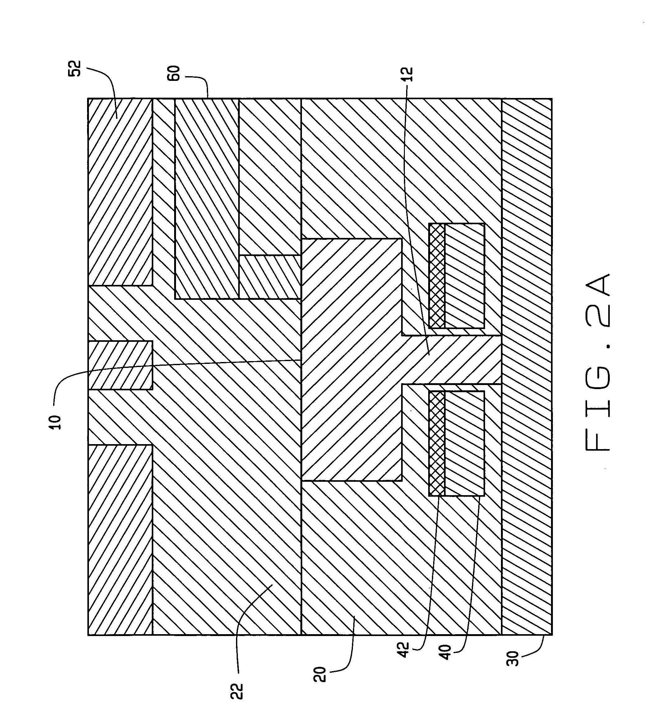
[0013] Referring to the drawings, FIGS. 1A and 1B schematically illustrate a photonic device 9 comprising a semiconductor substrate 30 and an overlying layer, such as insulating layer 20, including at least one semiconductor photoresponsive component 10. The substrate 30 includes at least one circuit component such as an insulated-gate field effect transistor including a source and a drain (not shown) underlying an insulated gate 40.

[0014] The photoresponsive component 10 advantageously overlies transistor insulated gate 40, and the gate 40 advantageously includes a layer 42 to prevent light that passes through the component 10 from entering the transistor region underlying the gate 40. Advantageously, the layer 42 also reflects the light back into the photoresponsive component 10.

[0015] In a preferred embodiment, the substrate 30 comprises single crystal silicon, the gate comprises polysilicon, the gate insulator comprises silicon oxide, and the layer 42 comprises metal silicide....


PUM


Abstract

In accordance with the invention, a photonic device comprises a semiconductor substrate including at least one circuit component comprising a metal silicide layer and an overlying layer including at least one photoresponsive component. The metal silicide layer is disposed between the circuit component and the photoresponsive component to prevent entry into the circuit component of light that penetrates the photoresponsive component. The silicide layer advantageously reflects the light back into the photoresponsive element. In addition, the overlying layer can include one or more reflective layers to reduce entry of oblique light into the photoresponsive component. In an advantageous embodiment, the substrate comprises single-crystal silicon including one or more insulated gate field effect transistors (IGFETs), and/or capacitors, and the photoresponsive element comprises germanium and/or germanium alloy epitaxially grown from seeds on the silicon. The metal silicide layer can comprise the gate of the IGFET and/or an electrode of the capacitor.

Description

STATEMENT OF GOVERNMENT INTEREST [0001] The United States Government has certain rights in this invention pursuant to NSF Phase II SBIR Award DMI-0450487.CROSS-REFERENCE TO RELATED APPLICATIONS Field of the Invention [0002] This invention relates generally to semiconductor photonic devices such as photodetectors for visible and infrared light. In particular, it concerns semiconductor dual layer photonic devices configured to enhance responsivity while reducing stray light. BACKGROUND OF THE INVENTION [0003] Semiconductor photonic devices are highly useful in a variety of applications ranging from monitoring, analyzing and imaging light to the generation of energy from solar radiation. Typically such devices comprise semiconductor photoresponsive components such as photodiodes, photoransistors or photoresistors integrated with semiconductor processing circuitry. Such devices can be used as photodetectors and solar cells. [0004] Semiconductor photodetectors are widely used for the det...

Claims


Application Information

Patent Timeline
IPC IPC(8): H01L31/06
CPCH01L27/14623H01L27/14685H01L31/02164H01L21/02639H01L21/02532H01L21/0262H01L21/02381H01L21/2018
Inventor RAFFERTY, CONOR S.KING, CLIFFORD ALAN
Owner INFRARED NEWCO
Why Eureka
Try Eureka