

High-frequency circuit and high-frequency device
- Summary
- Abstract
- Description
- Claims
- Application Information
AI Technical Summary
Benefits of technology
Problems solved by technology
Method used
Image

Examples
first embodiment
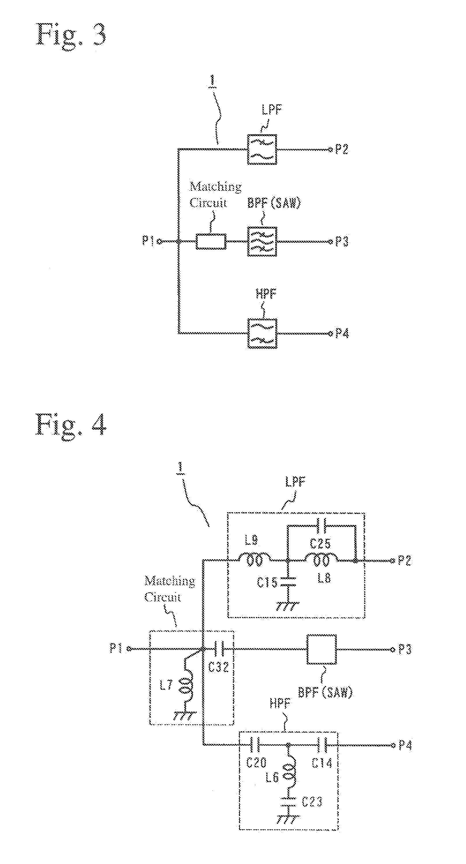
[0056]FIG. 8 shows a high-frequency device comprising the high-frequency circuit of FIG. 2 formed in a laminate substrate, and FIG. 9 shows the structures of the laminated layers. Symbols in FIG. 9 correspond to those in FIG. 2. Circuit elements not shown in FIG. 9 are mounted onto the laminate substrate as shown in FIG. 8.
[0057] A high-frequency device having the same equivalent circuit as that of the high-frequency circuit shown in FIG. 2 is a one-chip diplexer comprising part of inductance elements and capacitance elements constituting a lowpass filter circuit, a highpass filter circuit and a matching circuit, which are formed by electrode patterns formed on sheets in a laminate substrate, and the remaining part of the inductance elements and the capacitance elements and a SAW filter mounted onto the laminate substrate as chip parts. This high-frequency device is adapted to DAMPS as a first communications system, GPS as a second communications system, and PCS as a third communic...
second embodiment
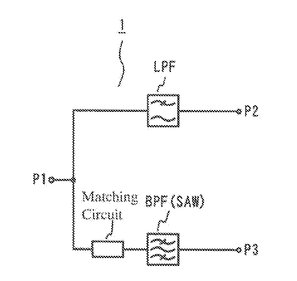
[0068]FIG. 11 shows a high-frequency circuit according to another embodiment of the present invention. This high-frequency circuit is suitably used for multi-band mobile phones comprising high-frequency devices as in the first embodiment. The high-frequency device 1 comprises a first port P1 connected to a multi-band antenna ANT, a second port P2 connected to a switch circuit SW for switching the paths of transmitting / receiving signals of DAMPS, and a fourth port P4 connected to a switch circuit SW for switching the paths of transmitting / receiving signals of PCS. A lowpass filter circuit LPF is disposed in each transmitting path for DAMPS and PCS, and a bandpass filter circuit BPF is disposed in each receiving path for DAMPS and PCS.
[0069] A third port P3, both lowpass filter circuits LPF and both bandpass filter circuits BPF of the high-frequency device 1 are connected to an amplifier circuit RFIC, which comprises a low-noise amplifier for amplifying and sending receiving signals ...
third embodiment
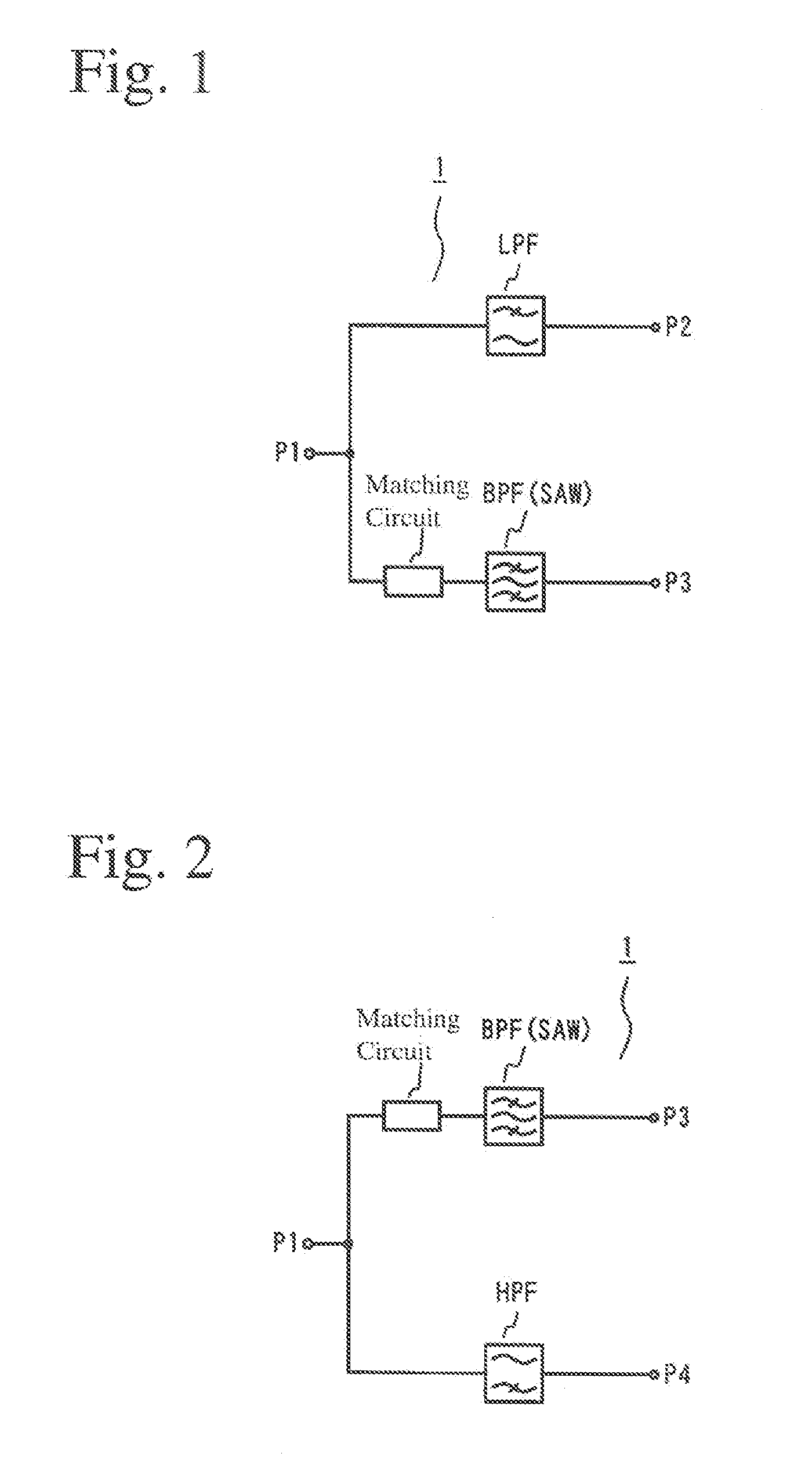
[0073]FIG. 12 shows a high-frequency circuit according to a further embodiment of the present invention. This high-frequency circuit is suitable for multi-band mobile phones comprising high-frequency devices as in the first embodiment. The high-frequency circuit of the third embodiment differs from that of the second embodiment, in that a single-pole, triple-throw (SP3T) switch circuit SW for switching paths for the transmitting / receiving signals of GSM and DAMPS is connected to a second port P2, that a single-pole, double-throw (SPDT) switch circuit SW for switching paths for the transmitting / receiving signals of WLAN is connected to a fourth port P4, that a lowpass filter circuit LPF or a bandpass filter circuit BPF is connected to the transmitting paths of DAMPS / GSM and WLAN, that bandpass filter circuits BPF are connected to the receiving paths of DAMPS / GSM and WLAN, and that circuits for performing convert between balanced and unbalanced signals Balun are connected between the ...
PUM
 Abstract
Description
Claims
Application Information