Method of producing optical element
a technology of optical elements and optical elements, applied in the direction of polycrystalline material growth, crystal growth process, chemically reactive gas, etc., to achieve the effect of reducing the amount of pb contained in the resulting optical element or completely removing i
- Summary
- Abstract
- Description
- Claims
- Application Information
AI Technical Summary
Benefits of technology
Problems solved by technology
Method used
Image
Examples
example 1
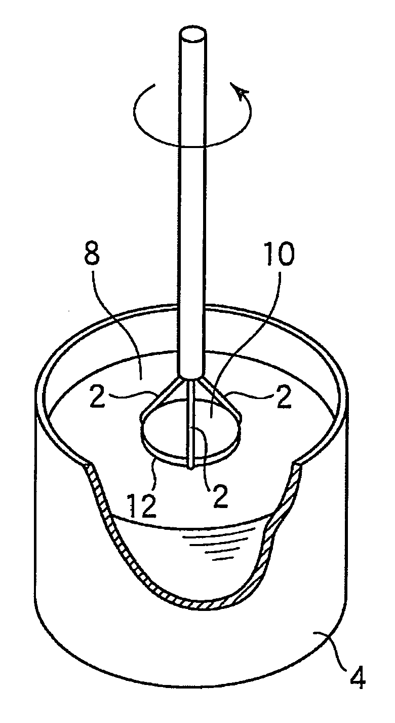
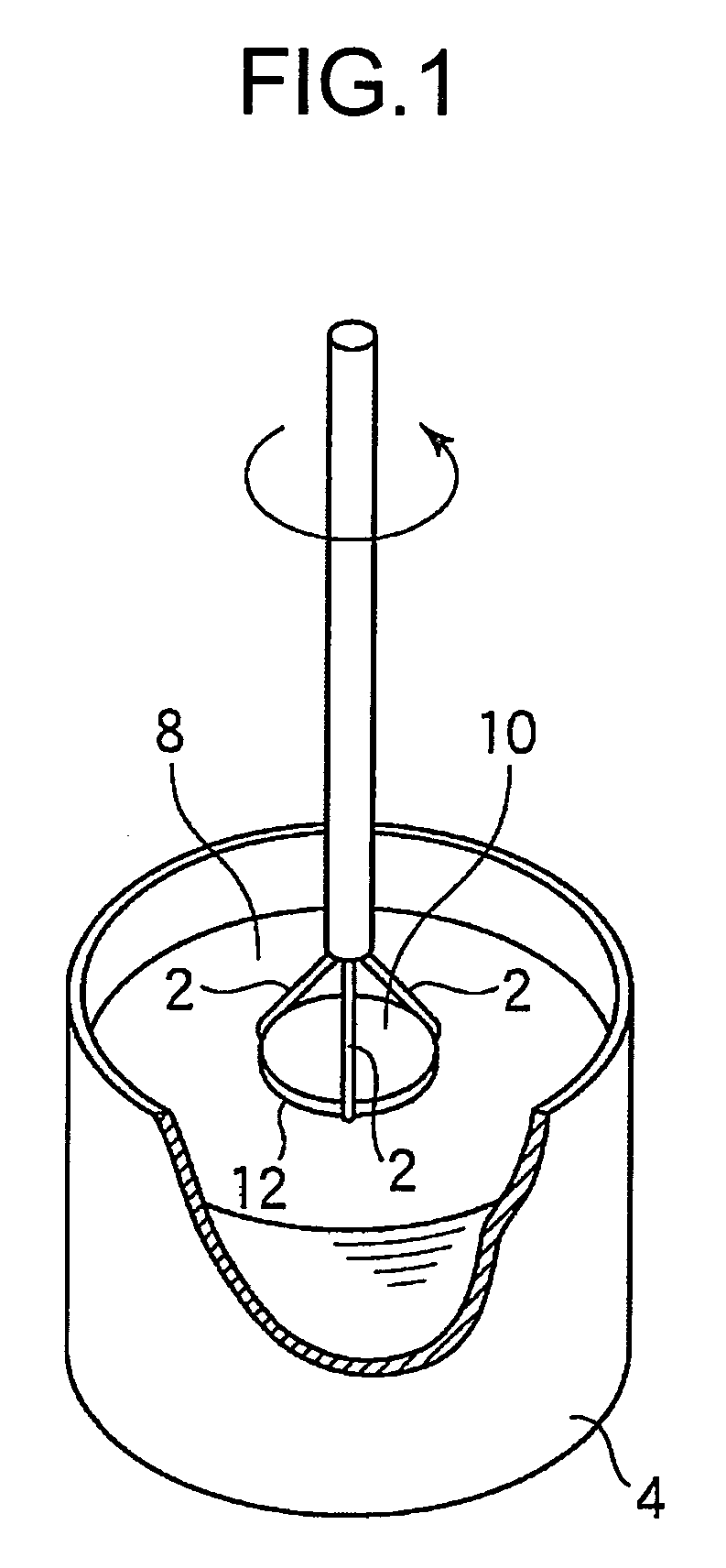
[0024]FIG. 1 depicts a part of the process of growing a single crystal in the present Example. Gd2O3, Yb2O3, Fe2O3, B2O3, Bi2O3, and NaOH were charged in a total weight of 2.3 kg in a crucible 4 made of gold (Au). The blended Fe ratio was 15.5 mol %. The blended ratios of B, Bi and Na were 7.0 mol %, 51.6 mol % and 25.4 mol %, respectively. Herein, the term “blended ratio” to be used in the specification represents the ratio of each element in molar number occupying the total molar number of elements (Na, Bi, B, Fe, rare-earth elements, and the like) becoming cations in a solution charged in the crucible 4. The crucible 4 with the materials charged therein was arranged in an electric furnace. By melting and agitating the materials in the crucible 4 by raising the furnace temperature to 900° C., a homogenous melt (solution) 8 was generated. Arranging a CaMgZr-substituted GGG (gadolinium gallium garnet) [(GdCa)3(GaMgZr)5O12] single crystal substrate 10 of a 2-inch diameter onto a fixi...
example 2
[0026] Gd2O3, Yb2O3, Fe2O3, B2O3, Bi2O3, and NaOH were charged in a total weight of 2.3 kg in a crucible 4 made of Au. The blended Fe ratio was 15.5 mol %. The blended ratios of B, Bi and Na were 7.0 mol %, 51.6 mol % and 25.4 mol %, respectively. The crucible 4 with the materials charged therein was arranged in an electric furnace. By melting and agitating the materials in the crucible 4 by raising the furnace temperature to 900° C., a homogenous melt 8 was generated. Arranging a CaMgZr-substituted GGG single crystal substrate 10 of a 2-inch diameter onto a fixing device 2, the substrate was charged in a furnace. After the temperature of the melt 8 was lowered down to 770° C., a single face of the substrate 10 was put in contact with the melt 8 to allow epitaxial growth for 40 hours. Consequently, a single crystal film 12 of a film thickness of 500 μm was grown. The single crystal was compositionally analyzed by X-ray fluorescence analysis. The composition was Bi1.00Gd1.70Yb0.30Fe5...
example 3
[0028] Gd2O3, Yb2O3, Fe2O3, B2O3, Bi2O3, and NaOH were charged in a total weight of 2.3 kg in a crucible 4 made of Au. The blended Fe ratio was 15.5 mol %. The blended ratios of B, Bi and Na were 7.0 mol %, 51.6 mol % and 25.4 mol %, respectively. The crucible 4 with the materials charged therein was arranged in an electric furnace. By melting and agitating the materials in the crucible 4 by raising the furnace temperature to 900° C., a homogenous melt 8 was generated. Arranging a CaMgZr-substituted GGG single crystal substrate 10 of a 2-inch diameter onto a fixing device 2, the substrate was charged in a furnace. After the temperature of the melt 8 was lowered down to 770° C., a single face of the substrate 10 was put in contact with the melt 8 to allow epitaxial growth for 40 hours. Consequently, a single crystal film 12 of a film thickness of 500 μm was grown. The single crystal was compositionally analyzed by X-ray fluorescence analysis. The composition was Bi1.00Gd1.70Yb0.30Fe5...
PUM
| Property | Measurement | Unit |
|---|---|---|
| wavelength | aaaaa | aaaaa |
| weight | aaaaa | aaaaa |
| temperature | aaaaa | aaaaa |
Abstract
Description
Claims
Application Information

