Topside Thermal Management of Semiconductor Devices

a topside heat sinking and semiconductor technology, applied in semiconductor devices, semiconductor/solid-state device details, electrical devices, etc., can solve the problems of limiting the effect of additional topside heat sinking, current approaches do not yet offer optimal thermal management, and the demands are literally daily increased, so as to improve thermal management and improve thermal management.

Inactive Publication Date: 2007-08-23
LOCKHEED MARTIN CORP
View PDF7 Cites 7 Cited by
  • Summary
  • Abstract
  • Description
  • Claims
  • Application Information

AI Technical Summary

Benefits of technology

[0009] Embodiments of the invention are directed to semiconductor devices having structural features that provide improved thermal management (e.g., heat dissipation), and to methods for obtaining improved thermal management in such devi

Problems solved by technology

For example, the air bridges are thermally far removed from the heat dissipating area of the die, which limits the effect of additional top

Method used


Image

  • Topside Thermal Management of Semiconductor Devices
  • Topside Thermal Management of Semiconductor Devices
  • Topside Thermal Management of Semiconductor Devices

Examples


example 1a

Baseline Thermal Impedance in SiC Substrate with 10 W / mm Output

[0025]

Output StageOutput Power density10 W / mmGate Width0.5 mmGate Pitch0.07 mmGate Length0.0004 mmHeatsink Temp100 deg C.Chip thickness0.1 mmCalibration temp25 deg C.Gain drift−0.015 dB / deg C.ss gain9.5 dBGain Compression2 dBefficiency65%Thermal conductivity0.268 w / mm-deg C.Theta Chip15.3 deg C. / WSingle Gate PD3.84 WDelta T chip58.9 deg C.T chip158.9 deg C.Gain correction−1.125Input power density2.30 W / mm

[0026] Note that the gate length is equal to 0.0004 mm and the calculated chip temperature Tchip equal to 158.9° C.

example 1b

Improved Thermal Impedance in SiC Substrate with 10 W / mm Output

[0027]

Output Stageoutput power density10 W / mmGate Width0.5 mmGate pitch0.07 mmEff. Gate Length0.0354 mmHeatsink Temp100 deg C.Chip thickness0.1 mmCalibration temp25 deg C.Gain drift−0.015 deg C.ss gain9.5 dBgain compression2 dBefficiency65%Thermal conductivity0.268 w / mm deg C.Theta chip8.90 deg C. / WSingle gate PD3.84 WDelta T chip34.2 deg C.T chip134.2 deg C.Gain correction−1.125Input power density2.30 W / mm

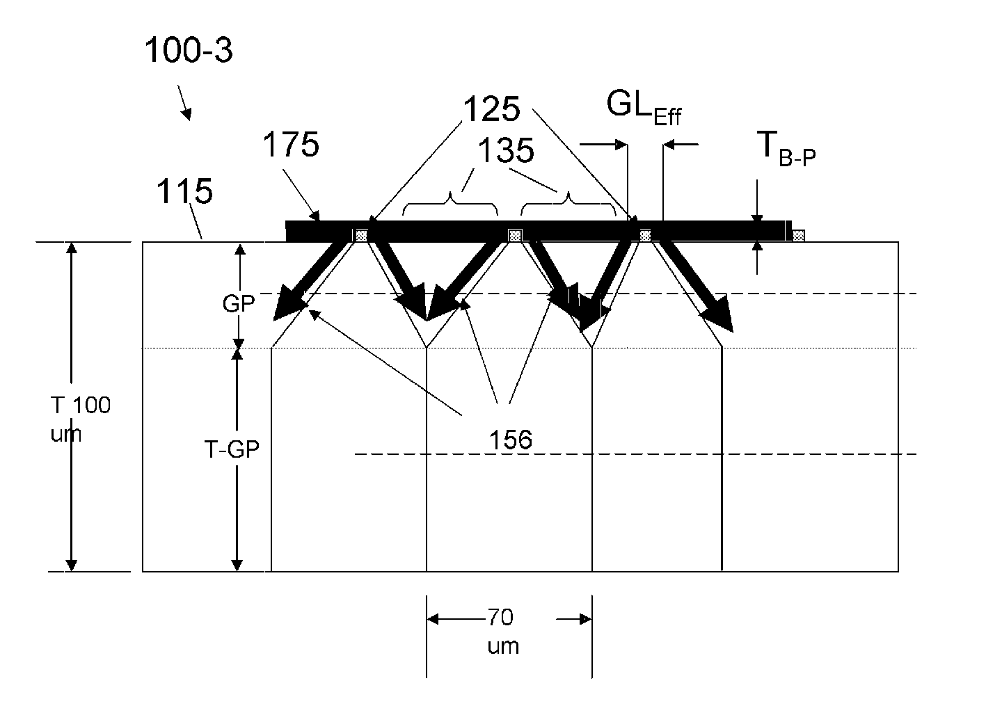
[0028] The effective gate length GLEFF increased to 0.0354 mm from the actual gate length GL of 0.0004 mm (Example 1a) due to the simulated boron phosphide coating as illustrated in FIG. 3A. The calculated chip temperature Tchip became 134.2° C. The thermal improvement, expressed as the difference in the chip temperatures, was about 25° C.

example 2a

Baseline Thermal Impedance in GaAs Substrate with 0.7 W / mm Output

[0029]

Output Stageoutput power Density0.7 W / mmGate Width0.5 mmGate pitch0.032 mmGate Length0.0005 mmHeatsink Temp80 deg C.Chip thickness0.1 mmCalibration temp25 deg C.Gain drift−0.015 dB / deg C.ss gain11 dBgain compression4 dBefficiency52%Thermal conductivity0.04 w / mm-deg C.Theta chip175.2 deg C. / WSingle gate PD0.408 WDelta T chip71.4 deg C.T chip151.4 deg C.Gain correction−0.825input power0.169 W / mmdensity

[0030] Note the actual gate length equal to 0.0005 mm and the chip temperature equal to 151.4° C.


PUM


Abstract

A semiconductor device including at least one gate terminal in operational contact with an active layer or top surface of the semiconductor substrate includes a deposited layer of boron phosphide covering the gate terminal and at least a portion of the active layer or the top surface next to and extending from the gate terminal. According to an aspect, the layer of boron phosphide is deposited by a chemical vapor deposition (CVD) process. The boron phosphide layer will have a thickness less than or equal to about 10 microns. The boron phosphide provides a heat spreading coating across the die surface, thus increasing the surface area that conducts the heat from the die. Since the boron phosphide coating is in intimate contact with the gate terminal(s) and the immediately adjacent passivation surfaces of the device, generated heat can rapidly spread away from the active junction or channel. The additional thermal path(s) provided by the boron phosphide coating may terminate away from the active region to further conduct away the heat through thermally unused areas of the device.

Description

BACKGROUND OF THE INVENTION [0001] 1. Field of the Invention [0002] Embodiments of the invention are generally directed to the field of semiconductors. More particularly, embodiments of the invention are directed to semiconductor devices having improved thermal characteristics and methods associated therewith. Most particularly, embodiments of the invention are directed (but not limited) to gallium nitride (GaN)-based monolithic microwave integrated circuits (MMICs) exhibiting improved heat dissipation and to methods for obtaining improved thermal performance from such devices. [0003] 2. Description of Related Art [0004] MMICs are semiconductor devices that are increasingly being used in radar, communications, antenna and sensor applications, as well as others, which demand small size and high performance. Various semiconductor technologies have been developed over the past 30 years. Persons skilled in the art will recognize these technologies to include Field Effect Transistor (FET...

Claims


Application Information

Patent Timeline
IPC IPC(8): H01L29/76
CPCH01L23/3735H01L29/66068H01L29/66462H01L2924/3011H01L2924/0002H01L2924/00
Inventor ROBINSON, KEVIN
Owner LOCKHEED MARTIN CORP
Why Eureka
Try Eureka