Line edge roughness reduction

a technology of etched substrates and rough edges, applied in the field of etching substrate methods, can solve the problems of undesirable effects of integrated circuit components, the inability so as to reduce the roughness of etched substrates

Inactive Publication Date: 2007-08-23
MICRON TECH INC
View PDF9 Cites 28 Cited by
  • Summary
  • Abstract
  • Description
  • Claims
  • Application Information

AI Technical Summary

Benefits of technology

[0007] Embodiments of the present disclosure include methods for reducing line edge roughness of etched substrates. One embodiment includes forming a masking structure on a substrate assembly that has a number of layers, forming a layered masking structure by depositing a layer of material on the masking structure in order to reduce a line edge roughness (LER) of the masking structure, and etching a pattern of the layered masking structure into one or more of the number of layers of the substrate assembly before trimming the layered masking structure.

Problems solved by technology

However, photolithographic methods are subject to line edge roughness (LER).
However, as device dimensions and, accordingly, mask features get smaller, the walls of masks and / or features etched therefrom can become intolerably rough.
The line edge roughness can result in undesirable effects in integrated circuit components, such as transistor leakage, for example.
LER effects can become more of a problem as the critical dimensions of transferred patterns become increasingly smaller.
However, such approach does not adequately improve sidewall LER, reduces, or “trims,” the thickness of the photoresist mask features, and can form breaks in long-running masking features, such as in parallel lines.

Method used


Image

  • Line edge roughness reduction
  • Line edge roughness reduction
  • Line edge roughness reduction

Examples


Embodiment Construction

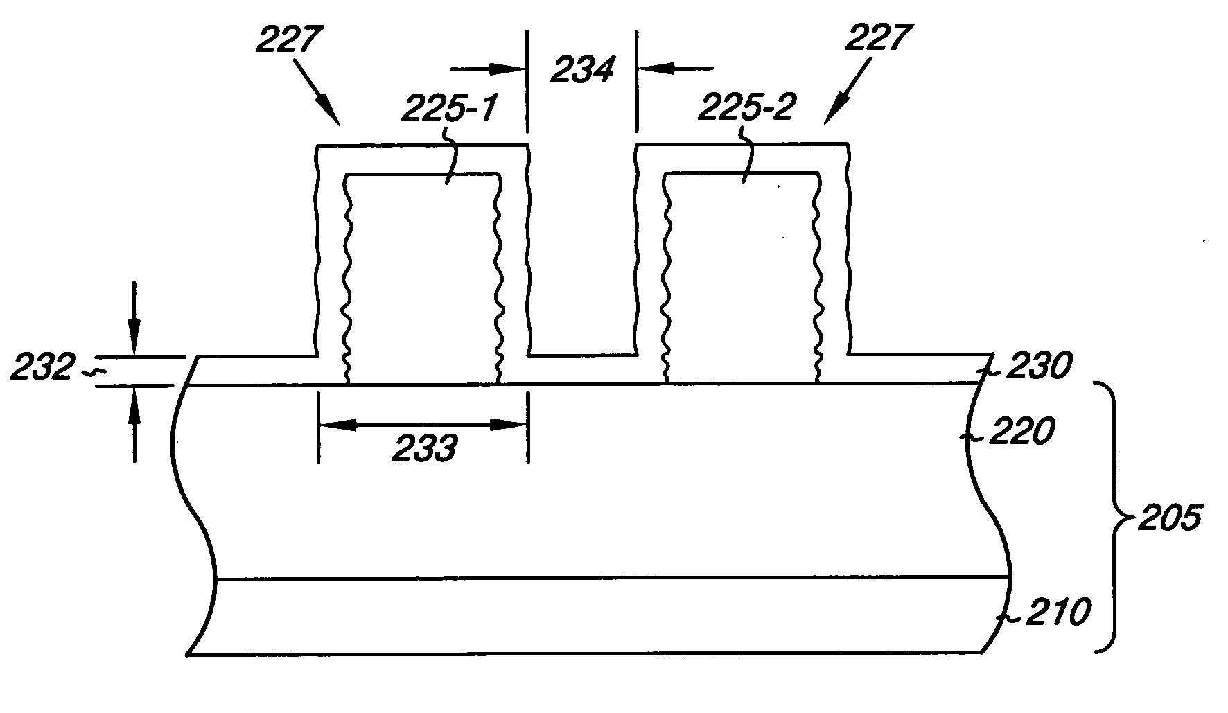
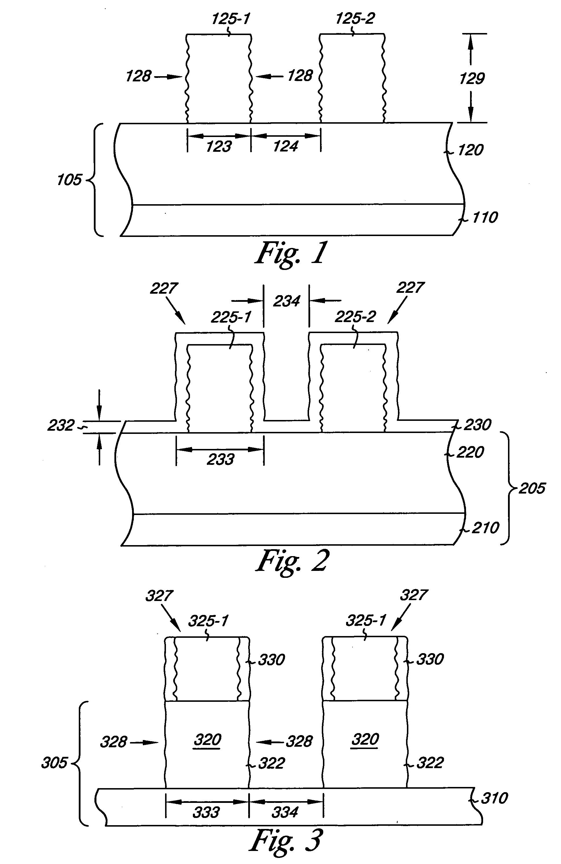
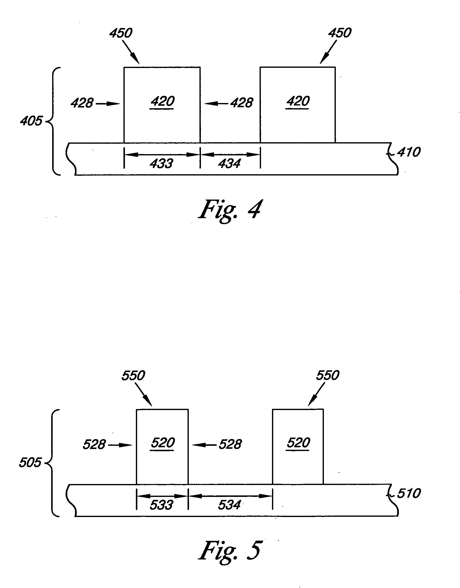
[0026]“Substrate” or “substrate assembly,” as used herein, refers to a semiconductor substrate such as a base semiconductor layer or a semiconductor substrate having one or more layers, structures, or regions formed thereon. A base semiconductor layer may be the lowest layer of silicon material on a wafer or a silicon layer deposited on another material, such as silicon on sapphire or silicon on insulator, among other examples.

[0027]“Layer” as used herein can refer to a layer formed on a substrate using a deposition process. The term “layer” is meant to include layers specific to the semiconductor industry, such as “barrier layer,”“dielectric layer,” and “conductive layer.” (The term “layer” is synonymous with the term “film” frequently used in the semiconductor industry). The term “layer” is also meant to include layers found in technology outside of semiconductor technology, such as coatings on glass. In the context of this document, the term “layer” encompasses both the singular...


PUM


Abstract

A method for reducing line edge roughness comprises forming a masking structure on a substrate assembly, wherein the substrate assembly includes a number of layers. The method includes forming a layered masking structure by depositing a layer of material on the masking structure in order to reduce a line edge roughness (LER) of the masking structure, and etching a pattern of the layered masking structure into one or more of the number of layers of the substrate assembly before trimming the layered masking structure.

Description

TECHNICAL FIELD [0001] The present disclosure relates to methods of etching substrates. More particularly, the present disclosure relates to etching methods used to reduce line edge roughness of patterned features by using a layered masking structure. BACKGROUND OF THE INVENTION [0002] In fabricating integrated circuit components, photolithographic patterning and etch can be used to transfer a desired pattern of a masking material, such as a photoresist, to an underlying substrate material or materials. The masking material pattern can include a series of spaced projections atop the underlying substrate material such that etching can thereby produce a corresponding series of spaced features in the underlying substrate material or materials. [0003] Advances in photolithography have enabled increasingly smaller patterns to be transferred into substrate materials, which can allow the formation of smaller integrated circuit components at lower cost. However, photolithographic methods ar...

Claims


Application Information

Patent Timeline
Patent Type & Authority Applications(United States)
IPC IPC(8): H01L21/8242
CPCH01L21/0337G03F7/40
Inventor SUBRAMANIAN, KRUPAKAR M.
Owner MICRON TECH INC
Why Eureka
Try Eureka