Nitride semiconductor component and process for its production

a technology of nitride and semiconductor components, applied in the direction of semiconductor devices, basic electric elements, electrical equipment, etc., can solve the problems of low commercial interest in inexpensive homoepitaxy of layer structure, increased production costs per component, and high dislocation concentration of gan layer on intermediate layer, etc., to achieve high compressive stress, large carrier wafers, and low cost of production

Active Publication Date: 2007-08-23
AZUR SPACE SOLAR POWER +1
View PDF8 Cites 113 Cited by
  • Summary
  • Abstract
  • Description
  • Claims
  • Application Information

AI Technical Summary

Benefits of technology

[0094]The advantage of the invention in this aspect is that particularly large carrier wafers can be used, since the process according to the invention can be carried out on large, commercially widely used silicon wafers. After removing the nitride semiconductor layer structure that has grown on the silicon wafer, the said structure can be bonded to a carrier wafer of corresponding size. The invention thus permits a particularly inexpensive production of components. The nitride semiconductor components in their totality may have for example a lateral dimension of at least 24 cm on the carrier.
[0095]Embodiments of the nitride semiconductor product according to the fourth aspect of the invention are described hereinafter, insofar as they do not follow directly from the previously described embodiments of the other aspects of the invention.
[0096]In a preferred embodiment the nitride semiconductor product has a curvature, measurable on the substrate in a direction perpendicular to the rear side substrate surface, that corresponds to a radius of curvature of at least 10 m or to an infinitely large radius of curvature. Such large radii of curvature are possible with the process procedures according to the invention if, due to the insertion of low-temperature strain engineering intermediate layers, a sufficiently high compressive stress is generated during the growth that is compensated as closely as possible in the subsequent cooling, due to the tensile stress that is then produced.

Problems solved by technology

On account of the very small size and poor quality of available substrates of nitride semiconductors there is at the present time little commercial interest in an inexpensive homoepitaxy of the layer structure of a nitride semiconductor component.
On the one hand they are expensive.
On the other hand commonly available substrates of these materials are comparatively small, so that the production costs per component are in addition increased on account of the relatively small yield for a given substrate surface.
A disadvantage of this technique is a high dislocation concentration in the GaN layer growing on the intermediate layer.
The fact is, on the one hand the SiN masking layer can, as its thickness increases, interfere with or even prevent the structural coupling between the AlN nucleation layer and the subsequently (i.e. after the SiN masking layer) growing GaN layer.
Secondly, a thick SiN layer increases the coalescence thickness to values that, with the known methods, can no longer be kept under the critical layer thickness for crack formation.
As a result, the insertion also of a SiN masking layer can accordingly no longer eliminate the tensile stress in the nitride semiconductor layer structure.
This problem also affects thin layer components such as thin layer LEDs, in which the silicon substrate is removed during the course of manufacture.
The processing of curved nitride semiconductor layer structure already cause problems and therefore increases the complexity and costs of component manufacture.
A curved nitride semiconductor layer structure that is then typically bonded to a carrier easily becomes detached from the carrier, and corresponding components have an undesirably short useful life.
The disadvantage here however is that tensile stresses still remain in the nitride semiconductor layer structure.
In addition this known LED has an undesirably high electrical resistance.

Method used


Image

  • Nitride semiconductor component and process for its production
  • Nitride semiconductor component and process for its production
  • Nitride semiconductor component and process for its production

Examples


Embodiment Construction

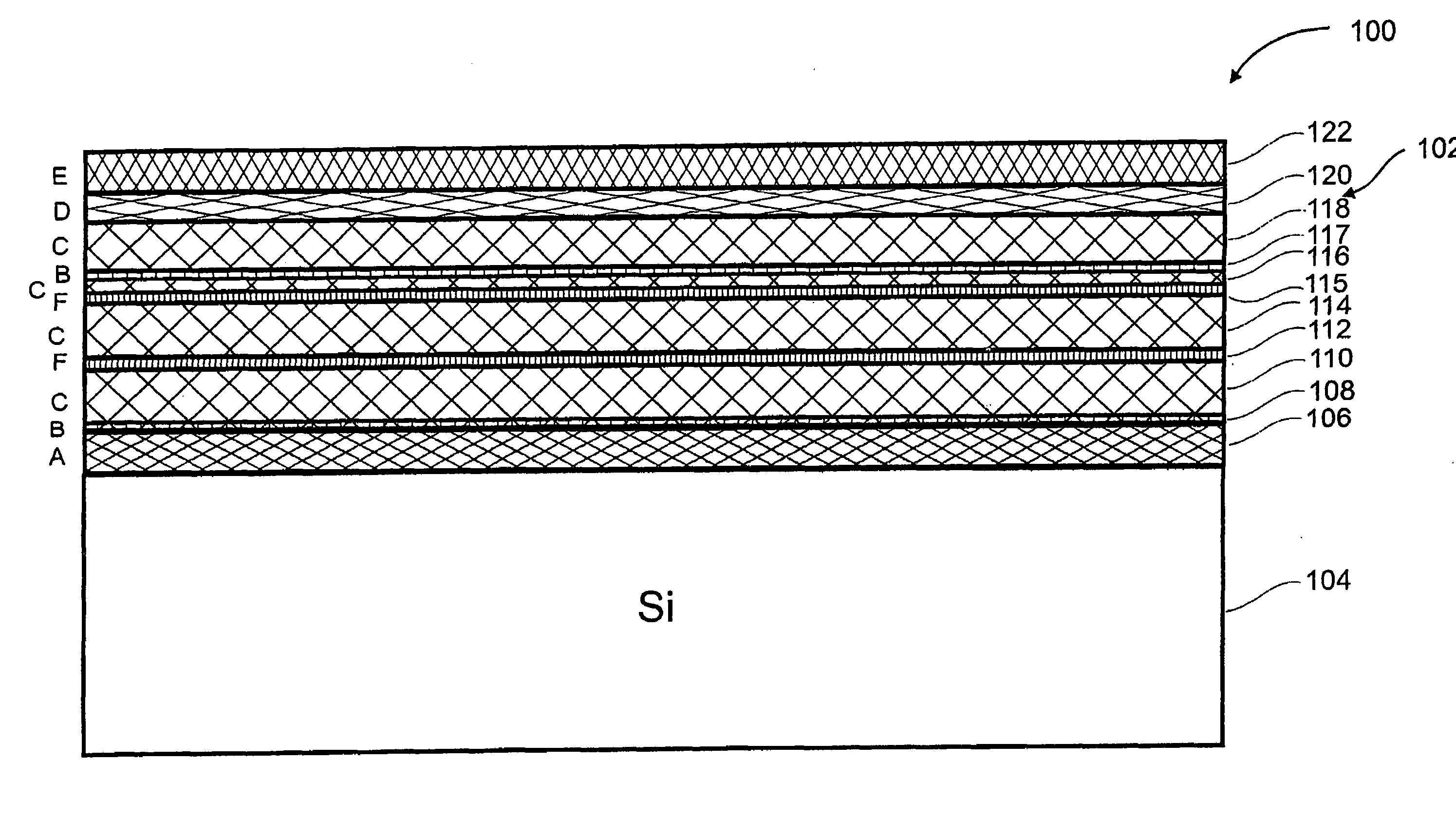
[0106]FIG. 1 shows in a diagrammatic view the layer structure of a nitride semiconductor product 100. The nitride semiconductor product 100 forms an intermediate product in the production of a nitride semiconductor component, as is explained in more detail hereinbelow with the aid of FIGS. 6a)-6f).

[0107]The illustration in FIG. 1 is not true to scale. In particular, the exact ratio of the layer thicknesses of the individual illustrated layers to one another cannot be determined from the figure. The layer thickness relationships shown in the figure thus provide only a fairly rough starting point. In the following description process aspects are discussed in parallel to device aspects on account of the lack of detail of the illustration.

[0108]The nitride semiconductor product 100 contains a layer structure 102 on a silicon wafer 104. The employed growth surface of the wafer, which is perpendicular to the plane of the paper of FIG. 1, is a (111) silicon surface. Instead of a silicon wa...


PUM

PropertyMeasurementUnit
surface areaaaaaaaaaaa
thicknessaaaaaaaaaa
thicknessaaaaaaaaaa

Abstract

The invention relates to a process for the production of a layer structure of a nitride semiconductor component on a silicon surface, comprising the steps:
    • provision of a substrate that has a silicon surface;
    • deposition of an aluminium-containing nitride nucleation layer on the silicon surface of the substrate;
    • optional: deposition of an aluminium-containing nitride buffer layer on the nitride nucleation layer;
    • deposition of a masking layer on the nitride nucleation layer or, if present, on the first nitride buffer layer;
    • deposition of a gallium-containing first nitride semiconductor layer on the masking layer,
wherein the masking layer is deposited in such a way that, in the deposition step of the first nitride semiconductor layer, initially separate crystallites grow that coalesce above a coalescence layer thickness and occupy an average surface area of at least 0.16 μm2 in a layer plane of the coalesced nitride semiconductor layer that is perpendicular to the growth direction.

Description

CROSS REFERENCE TO RELATED APPLICATION[0001]Reference is made to and priority claimed from U.S. provisional application Ser. No. 60 / 776,457 filed Feb. 23, 2006.BACKGROUND OF THE INVENTION[0002]1. Technical Field[0003]The present invention relates to a process for the production of a layer structure of a nitride semiconductor component on a silicon surface. The invention also relates to a process for the production of a nitride semiconductor component. Finally, the invention relates to a nitride semiconductor component, in particular a thin film light-emitting diode (LED) based on a nitride semiconductor, as well as a nitride semiconductor product.[0004]2. Discussion of Related Art[0005]Nitride semiconductors are semiconductor compounds that contain one or more elements of the third main group as well as one or more elements of the fifth main group of the Periodic System. Such semiconductors include for example the semiconductors GaN, InGaN, InGaAsN, AlGaN, etc. Other common designat...

Claims


Application Information

Patent Timeline
Patent Type & Authority Applications(United States)
IPC IPC(8): H01L21/20
CPCH01L21/02381H01L21/02458H01L21/02505H01L21/02647H01L21/0262H01L21/02639H01L21/0254H01L33/0093H01L33/007H01L33/06H01L33/24H01L33/32
Inventor DADGAR, ARMINKROST, ALOIS
Owner AZUR SPACE SOLAR POWER
Why Eureka
Try Eureka