Hybrid wafer-holder

a technology of silicon wafers and wafer holders, applied in the direction of electrical equipment, basic electric elements, electric discharge tubes, etc., can solve the problems of secure wafer gripping, wafers subject to relatively severe conditions, and conventional wafer holding devices are often incapable of withstand the relatively high temperatures associated with simox processing, etc., to reduce heat loss from the wafer

Inactive Publication Date: 2007-08-30
IBIS TECH
View PDF3 Cites 20 Cited by
  • Summary
  • Abstract
  • Description
  • Claims
  • Application Information

AI Technical Summary

Benefits of technology

[0026] In yet another aspect, a wafer-holding pin for use in an ion implanter can include a distal portion comprising a wafer-receiving groove, a proximal portion adapted for coupling with a wafer-holding assembly, and a thermally conductive insert disposed in said distal portion such that a surface portion of said insert provides an anchoring site for the wafer in the groove. The insert can further provide a thermal path for transferring heat to the wafer.
[0027] In a further aspect of the invention...

Problems solved by technology

During the SIMOX process, the wafers are subjected to relatively severe conditions.
Conventional wafer-holding devices are often incapable of withstanding the relatively high temperatures associated with SIMOX processing.
Besides the extreme temperature conditions, in rotatable ion implantation systems a secure wafer gripping problem arises.
Furthermore, wafer-holding structures having exposed metal are ill-suited for SIMOX processes because the ion beam will induce sputtering of the metal and, thus, result in wafer contamination.
In addition, the structure may deform asymmetrically due to thermal expansion, which can damage the wafer surface and/or edge during high temperature annealing so as to compromise wafer integrity and render it unusable.
Another disadvantage associated with certain known wafer holders is electrical discharge of the wafers.
The charge build up disrupts the implantation process by stripping the ion beam of space charge neutralizing electrons.
The charge built-up on the wafer can also result in a discharge to a nearby structure via an electrical arc, which can also contaminate the wafer or otherwise damage it.
Another disad...

Method used


Image

  • Hybrid wafer-holder
  • Hybrid wafer-holder
  • Hybrid wafer-holder

Examples


Embodiment Construction

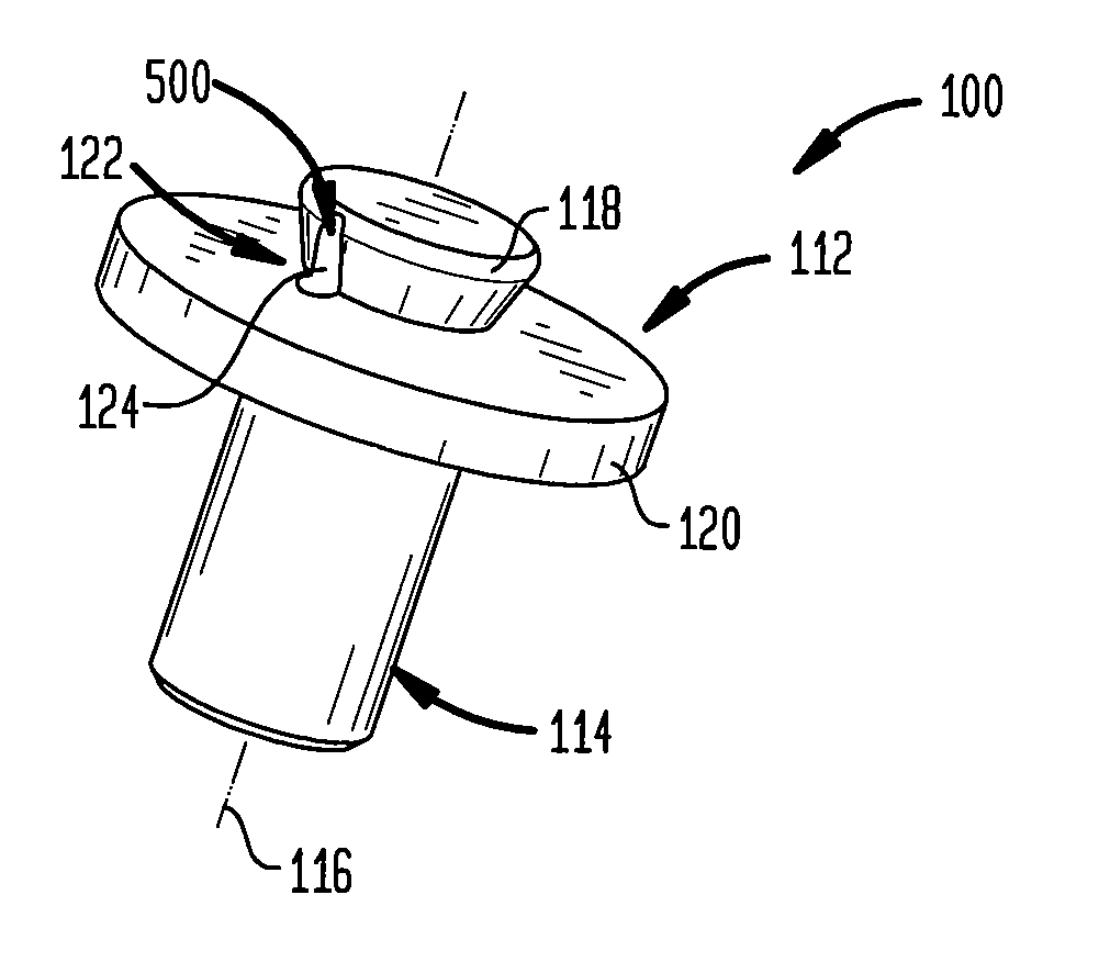
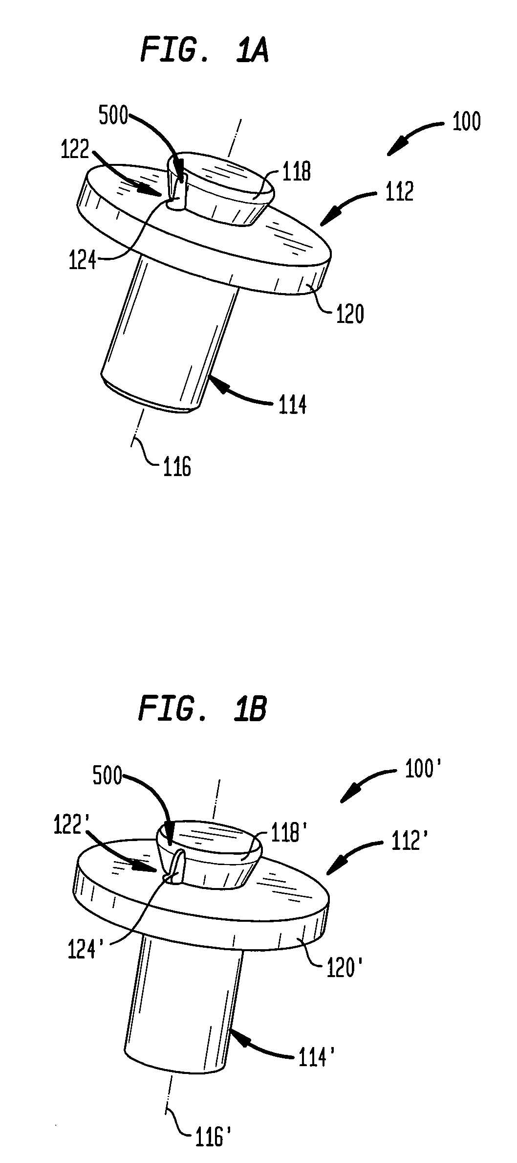
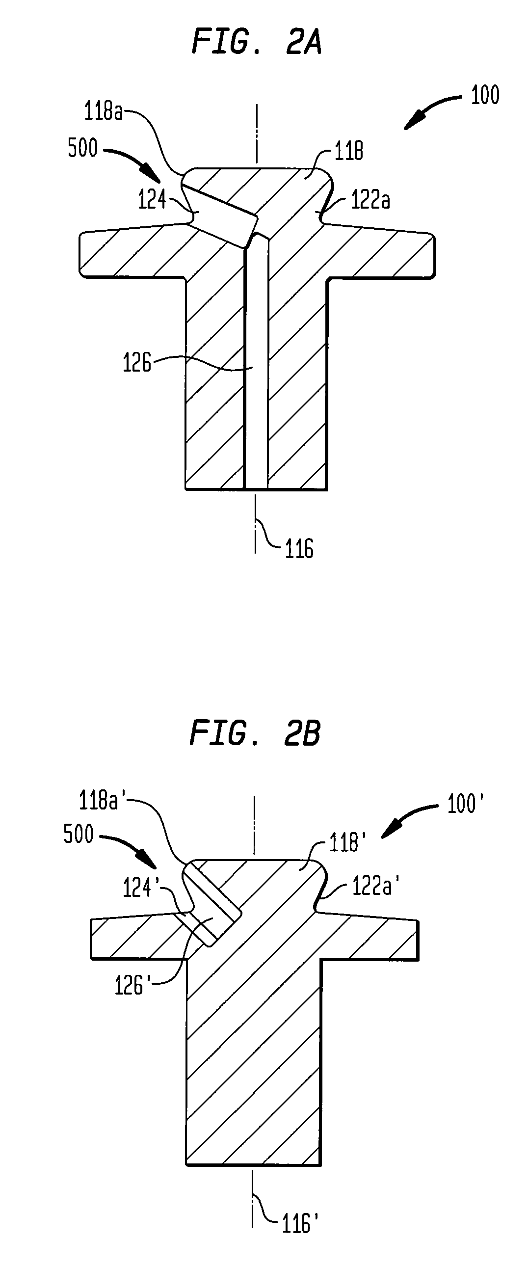
[0041] The present invention provides a wafer-holding pin that is well-suited for use with SIMOX wafer processing including use of relatively high ion beam energies and temperatures in a vacuum or reduced pressure environment. In general, the wafer-holding pin has a structure that maintains its integrity and reduces the likelihood of wafer damage during extreme conditions associated with SIMOX wafer processing. In some embodiments, the wafer-holding pin can be formed from a thermosetting resin that can be filled with a conductive material to provide an electrical path from the wafer to ground for preventing electrical charging of the wafer, and possible arcing, during the ion implantation process. Portions of the wafer-holding pin can be embedded with graphite to reduce wafer rotation during implantation.

[0042] Some embodiments provide wafer-holding pins that are formed of a thermosetting resin material impregnated with a conductive material, such as graphite, so as to provide an e...


PUM

PropertyMeasurementUnit
Temperatureaaaaaaaaaa
Angleaaaaaaaaaa

Abstract

Wafer-holding structures formed from thermosetting resins are disclosed for use in semiconductor processing including, for example, SIMOX wafer processing. At least a portion of the distal portion of the holder comprises graphite, thereby reducing wafer rotation during implantation while maintaining the desired overall thermal signature provided by the thermosetting resin. In one embodiment a pin is disclosed that is adapted to receive a wafer edge, and is coupled with a wafer holder assembly. The pin can be filled with a conductive material to provide an electrical pathway between the wafer and the wafer holder assembly, which can be coupled to a ground. This arrangement provides a conductive path for inhibiting electrical discharges from the wafer during the ion implantation process. The pin exhibits thermal isolation characteristics and sufficient hardness so as to not effect localized thermal dissipation of the wafer, yet is sufficiently soft so as to not mark or otherwise damage the wafer.

Description

RELATED APPLICATION [0001] The present invention claims priority to a provisional application entitled “Hybrid Wafer-Holder,” filed on Feb. 28, 2006 and having a Ser. No. 60 / 777,581. This provisional application is herein incorporated by reference in its entirety.BACKGROUND OF THE INVENTION [0002] The present invention relates generally to silicon wafer processing, and more particularly, to devices for holding silicon wafers as they are subjected to ion bombardment and to heat treatment. [0003] Various techniques are known for processing silicon wafers to form devices, such as integrated circuits. One technique includes implanting oxygen ions into a silicon wafer to form buried layer devices known as silicon-on-insulator (SOI) devices. In these devices, a buried insulation layer is formed beneath a thin surface silicon film. These devices have a number of potential advantages over conventional silicon devices (e.g., higher speed performance, higher temperature performance and increa...

Claims


Application Information

Patent Timeline
IPC IPC(8): H01L21/306
CPCH01J37/20H01J37/3171H01J2237/2007H01L21/68757H01L21/67213H01L21/68728H01L21/67103
Inventor LEAVITT, WILLIAMRICHARDS, STEVEN
Owner IBIS TECH
Why Eureka
Try Eureka