Piezoelectric thin film device

a thin film device and piezoelectric technology, applied in the field can solve problems such as the degradation and achieve the effect of improving the quality improving the characteristics of piezoelectric thin film devices

Inactive Publication Date: 2007-08-30
NGK INSULATORS LTD +1
View PDF1 Cites 21 Cited by
  • Summary
  • Abstract
  • Description
  • Claims
  • Application Information

AI Technical Summary

Benefits of technology

[0008]Thereby, it is possible to improve characteristics of the piezoelectric thin film device since the quality of the piezoelectric thin film can be improved.
[0009]Accordingly, an object of the present invention is to improve the characteristics of the piezoelectric thin film device.

Problems solved by technology

However, in the related art, it is difficult to construct the piezoelectric thin film 94 comprising a single-crystal piezoelectric material since the piezoelectric thin film 94 is formed on the lower electrode 93, which is a metal film, and there has thus been a problem in that characteristics of the piezoelectric thin film device deteriorate due to quality degradation of the piezoelectric thin film attributed to lowered crystallinity.

Method used


Image

  • Piezoelectric thin film device
  • Piezoelectric thin film device
  • Piezoelectric thin film device

Examples


first embodiment

1 First Embodiment

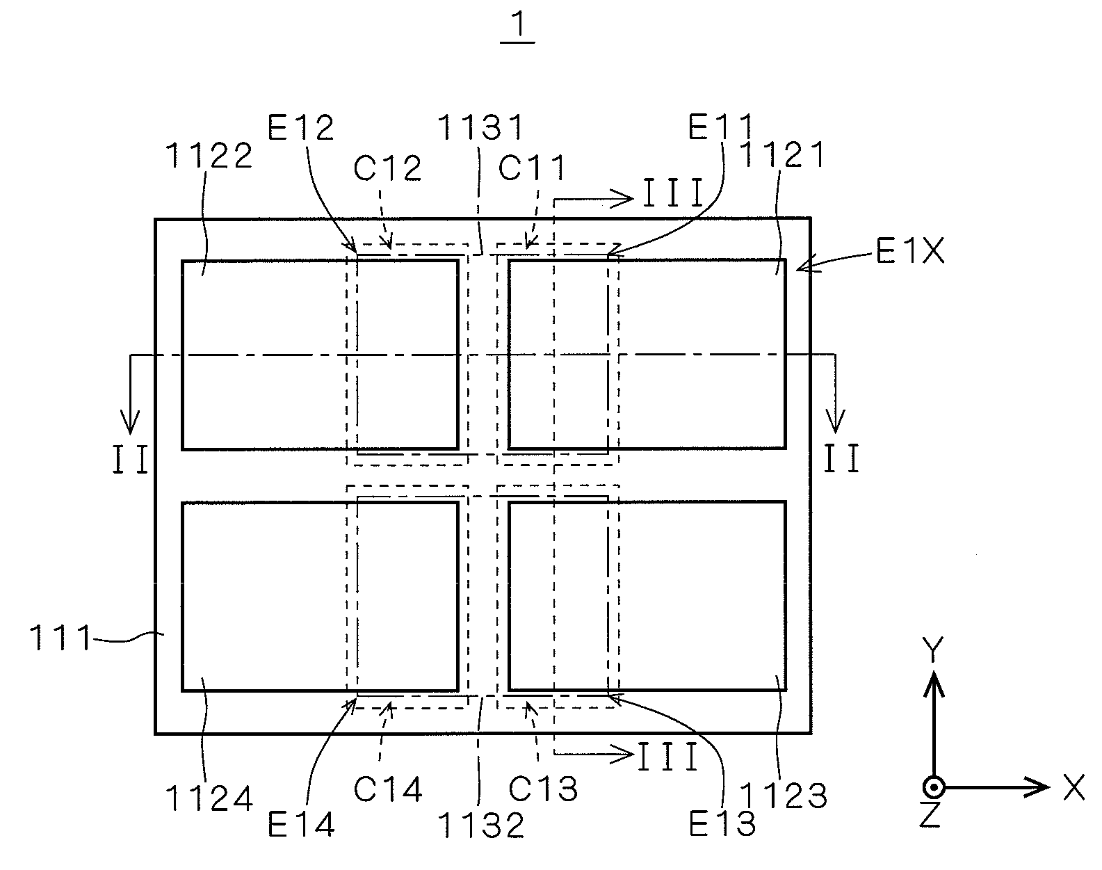
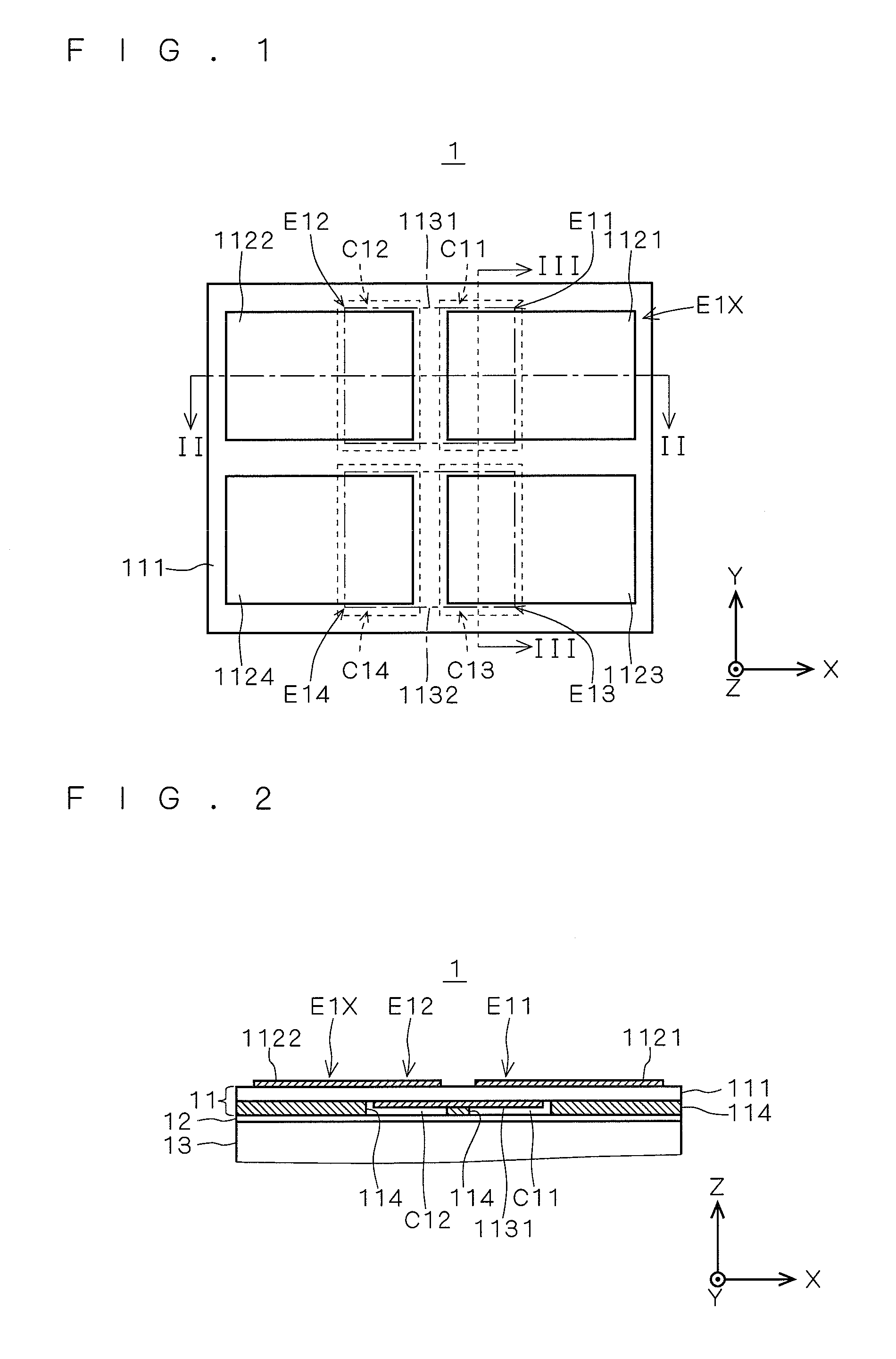
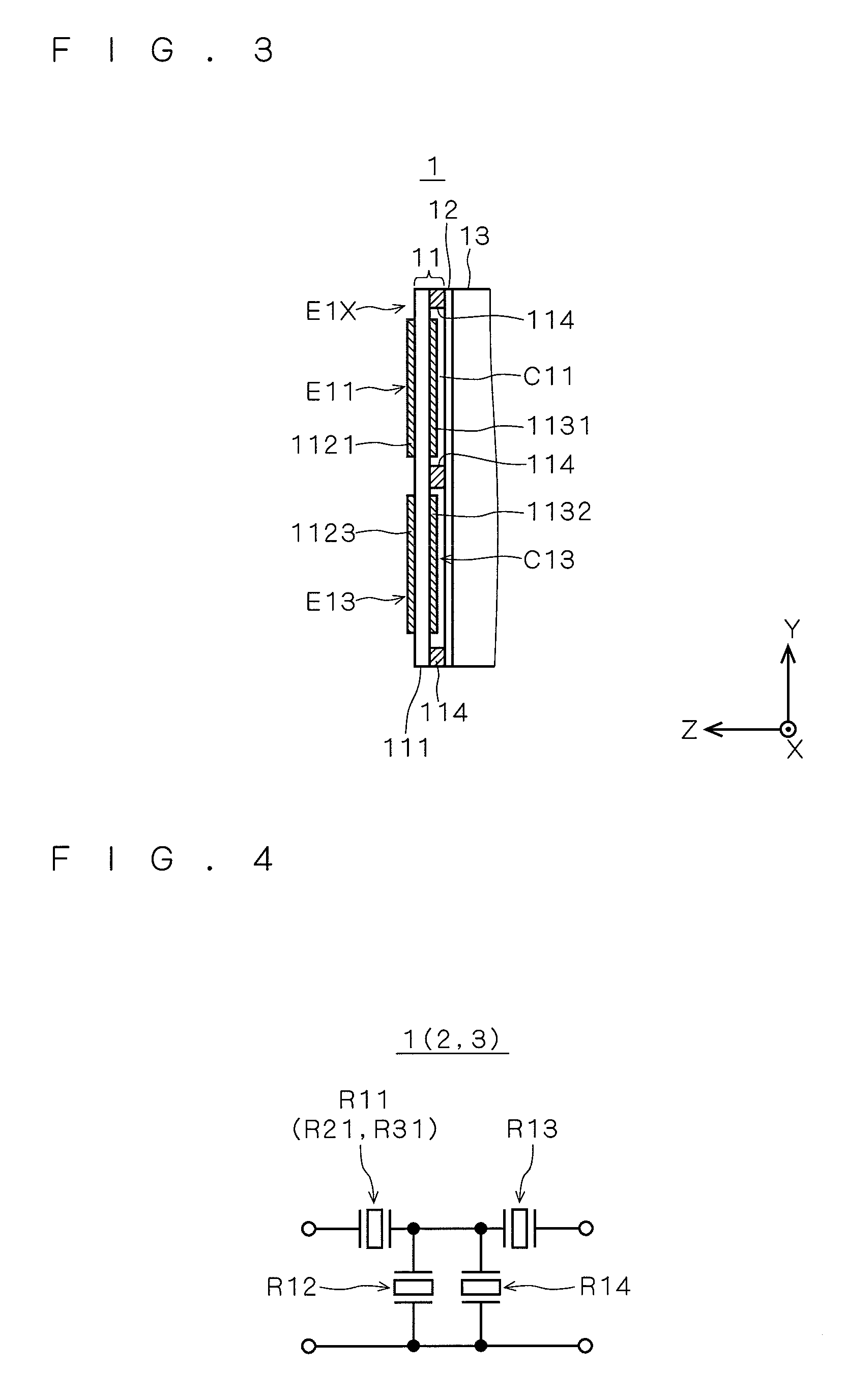
[0025]FIGS. 1 to 4 show a configuration of a piezoelectric thin film filter 1 according to a first embodiment of the present invention. FIG. 1 is a plan view of the piezoelectric thin film filter 1 seen from the top. FIG. 2 is a sectional pattern view along a cross section II-II of FIG. 1 seen from the front (−Y direction). FIG. 3 is a sectional pattern view along a cross section III-III of FIG. 1 seen from the right (+X direction). FIG. 4 is a circuit diagram showing an electric connection state of four film bulk acoustic resonators R11 to R14 included in the piezoelectric thin film filter 1. It is be noted that in FIGS. 1 to 3, an XYZ orthogonal coordinate system is defined for the sake of simplicity where the right-and-left direction is ±X-axis direction, the front-and-back direction is ±Y-axis direction, and the top- and bottom-direction is ±Z-axis direction.

[0026]As shown in FIGS. 1 to 3, the piezoelectric thin film filter 1 has a configuration where a filter ...

second embodiment

2 Second Embodiment

[0045]A piezoelectric thin film filter 2 according to a second embodiment of the present invention has a similar configuration to that of the piezoelectric thin film filter 1 according to Embodiment 1, but a cavity formation method for the piezoelectric thin film filter 2 differs from that for the piezoelectric thin film filter 1.

[0046]A description is made with a focus on one film bulk acoustic resonator R21 included in the piezoelectric thin film filter 2. As shown in a sectional pattern view of FIG. 5, the piezoelectric thin film filter 2 comprises: an upper electrode 2121; a piezoelectric thin film 211; a lower electrode 2131; an adhesive layer 22 and a base substrate 23, corresponding to the upper electrode 1121; the piezoelectric thin film 111; the lower electrode 1131; the adhesive layer 12 and the base substrate 13 respectively. Further, in the piezoelectric thin film filter 2, a lower electrode 2135 as a dummy electrode is formed on the bottom surface of ...

third embodiment

3 Third Embodiment

[0049]A piezoelectric thin film filter 3 according to a third embodiment of the present invention has a similar configuration to that of the piezoelectric thin film filter 1 according to Embodiment 1, but a cavity formation method for the piezoelectric thin film filter 3 differs from that for the piezoelectric thin film filter 1.

[0050]A description is made with a focus on one film bulk acoustic resonator R31 included in the piezoelectric thin film filter 3. As shown in a sectional pattern view of FIG. 6, the piezoelectric thin film filter 3 comprises: an upper electrode 3121; a piezoelectric thin film 311; a lower electrode 3131; an adhesive layer 32 and a base substrate 33, corresponding to the upper electrode 1121; the piezoelectric thin film 111; the lower electrode 1131; the adhesive layer 12 and the base substrate 13 respectively.

[0051]However, the piezoelectric thin film filter 3 does not have a configuration corresponding to that of the cavity formation film...


PUM


Abstract

The present invention is directed to improving characteristics of a piezoelectric thin film device. A piezoelectric thin film filter including four film bulk acoustic resonators has a configuration where a filter section and a base substrate are bonded to each other via an adhesive layer, the filter section including a piezoelectric thin film which cannot stand up individually under its own weight, the flat base substrate mechanically supporting the filter section. As a piezoelectric material constructing the piezoelectric thin film, it is desirable to use a single-crystal material including no grain boundary, selected from crystal, lithium niobate, lithium tantalite, lithium tetraborate, zinc oxide, potassium niobate, and langasite.

Description

BACKGROUND OF THE INVENTION[0001]1. Field of the Invention[0002]The present invention relates to a piezoelectric thin device including a single or a plurality of film bulk acoustic resonators (FBAR).[0003]2. Description of the Background Art[0004]A piezoelectric thin device including a single or a plurality of film bulk acoustic resonators, such as an oscillator, a trap, a filter, a duplexer and a triplexer, has hitherto been manufactured by sequentially forming, on a supporting layer 92 formed on a base substrate 91, a lower electrode 93, a piezoelectric thin film 94, and an upper electrode 95 by sputtering or the like, and then forming a cavity C91 below an excitation region E91 of the piezoelectric thin film 94 by etching or the like (e.g. see Japanese Patent Application Laid-Open No. 2005-94735).[0005]However, in the related art, it is difficult to construct the piezoelectric thin film 94 comprising a single-crystal piezoelectric material since the piezoelectric thin film 94 is ...

Claims


Application Information

Patent Timeline
Patent Type & Authority Applications(United States)
IPC IPC(8): H01L41/08H01L41/09H01L41/18H01L41/22H01L41/313H01L41/337H03H9/17H03H9/54
CPCH03H3/02H03H9/02023H03H9/02031H03H9/02039H03H2003/021H03H9/02133H03H9/173H03H9/564H03H9/02055H03H9/15H03H9/00
Inventor YOSHINO, TAKASHIYAMAGUCHI, SHOICHIROIWATA, YUICHIHAMAJIMA, AKIRASUZUKI, KENGO
Owner NGK INSULATORS LTD
Why Eureka
Try Eureka