Semiconductor device

a technology of semiconductor devices and semiconductors, applied in the direction of pulse techniques, process and machine control, instruments, etc., can solve the problems of large loss, increased frequency of shoot-through, and superfluous loss, so as to reduce the loss of power supplies, and reduce the effect of power supply loss

Inactive Publication Date: 2007-08-30
RENESAS ELECTRONICS CORP
View PDF10 Cites 57 Cited by
  • Summary
  • Abstract
  • Description
  • Claims
  • Application Information

AI Technical Summary

Benefits of technology

[0011]An object of the present invention is to provide a technique which can reduce a loss of a power supply having a large current and a high frequency.

Problems solved by technology

Since the high-side and low-side MOSFET are simultaneously turned on, a shoot-through current flows between an input power supply and a ground, and a superfluous loss is created.
Under a condition of high frequency, there is a problem that a frequency of the shoot-through is increased, and a great loss is caused.
However, since a ratio di / dt becomes larger due to the large current requirement and surge voltage at a time of turning on is increased in accordance therewith, countermeasures only by device structures are insufficient.

Method used


Image

  • Semiconductor device
  • Semiconductor device
  • Semiconductor device

Examples


embodiment 1

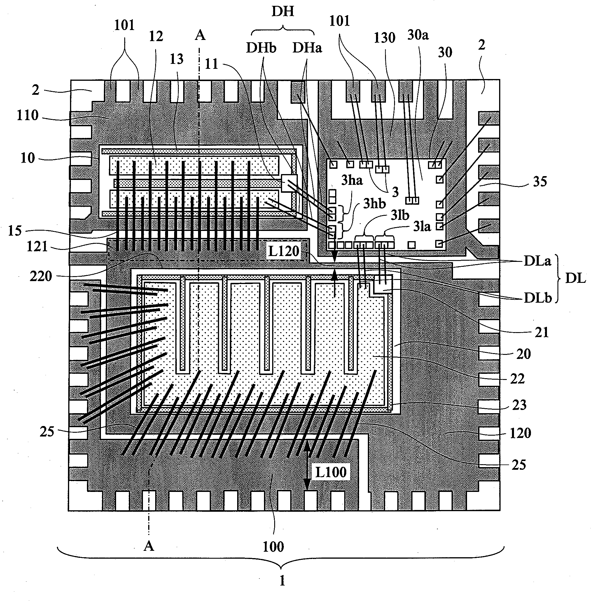
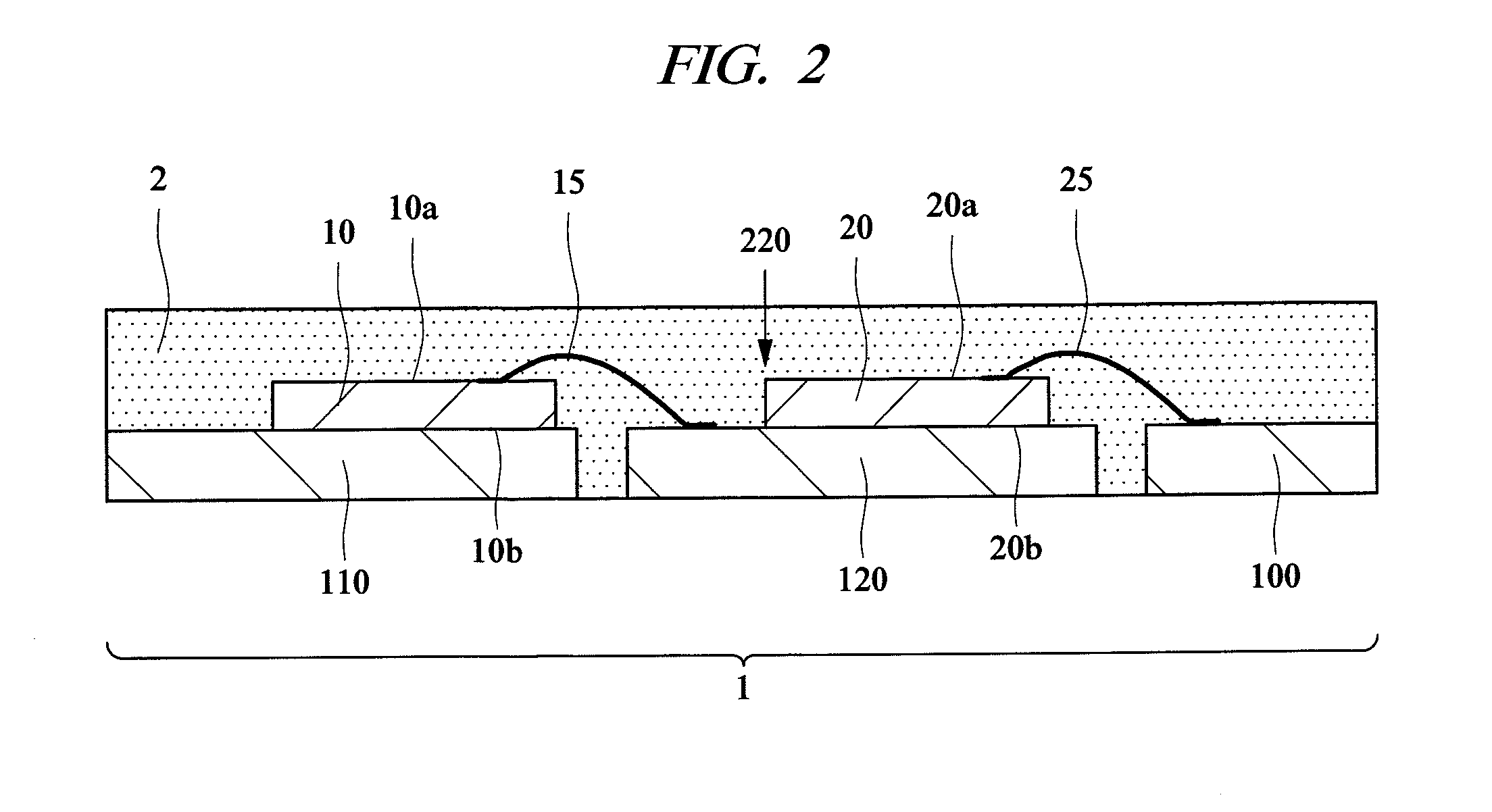
[0048]FIG. 1 is a plan view showing an MCM (multi-chip module) 1 corresponding to a semiconductor device according to an embodiment 1 of the present invention through a sealing material on a front surface thereof, FIG. 2 is a cross sectional view showing a structure of a cross section of the MCM cut along the line A-A shown in FIG. 1, FIG. 3 is a plan view showing a structure of a back surface of the MCM 1 shown in FIG. 1, FIG. 4 is a schematic cross sectional view showing a unit cell structure of an n-channel type vertical field effect transistor used in a high-side power MOSFET chip of the MCM 1, FIG. 5 is an outer appearance perspective view of the MCM 1, and FIG. 6 is a circuit diagram showing an example of an equivalent circuit of a non-isolated DC-DC converter using the MCM 1 shown in FIG. 1.

[0049]The semiconductor device according to the embodiment 1 shown in FIGS. 1 to 6 is structured such that a plurality of semiconductor chips are sealed in one sealing material (an isolati...

embodiment 2

[0128]FIG. 13 is a plan view showing an MCM 1c according to an embodiment 2 of the present invention with the sealing material on the front surface made transparent. In FIG. 13, a description of the same reference numerals as those of FIG. 1 is omitted.

[0129]A different point between the MCM 1c shown in FIG. 13 and the MCM 1 shown in FIG. 1 exists in a point that the convex region 121 in FIG. 1 is not provided within the output side plate lead portion 100, and the number of the wiring DL is larger than the number of the wiring DH (the number of the wiring DLa is three, the number of the wiring DLb is three, the number of the wiring DHa is two, and the number of the wiring DHb is two).

[0130]In the MCM 1c according to the present embodiment 2, since the convex region 121 shown in FIG. 1 is not provided, it is possible to make good use of the existing lead frame, however, since it is affected by the connection region between the source terminal 12 of the high-side power MOSFET chip 10 ...

embodiment 3

[0133]FIG. 14 is a plan view showing an MCM 1d according to an embodiment 3 of the present invention in such a manner with a sealing material on the front surface viewed transparent. In FIG. 14, a description of the same reference numerals as those of FIG. 1 is omitted.

[0134]A different point between the MCM 1d shown in FIG. 14 and the MCM 1 shown in FIG. 1 exists in a point that the number of the wiring DL is larger than the number of the wiring DH (the number of the wiring DLa is three, the number of the wiring DLb is three, the number of the wiring DHa is two, and the number of the wiring DLb is two). Since the convex region 121 is provided, the wiring DL is short. Further, since the numbers of the wirings DLa and DLb are increased from two to three, it is possible to reduce the combined parasitic inductance of the wirings DLa and DLb to about two thirds of the combined parasitic inductance of the wirings DLa and DLb of the MCM 1.

[0135]In this case, the description is given where...


PUM


Abstract

A power supply capable of reducing loss of large current and high frequency. In an MCM for power supply in which a high-side power MOSFET chip, a low-side power MOSFET chip and a driver IC chip driving them are sealed in one sealing material (a capsulating insulation resin), a wiring length of a wiring DL connecting an output terminal of the driver IC chip to a gate terminal of the low-side power MOSFET chip or a source terminal is made shorter than a wiring length of a wiring DH connecting the output terminal of the driver IC chip to a gate terminal of the high-side power MOSFET chip or a source terminal. Further, the number of the wiring DL is made larger than the number of the wiring DH.

Description

CROSS-REFERENCE TO RELATED APPLICATION[0001]The present application claims priority from Japanese Patent Application No. JP 2006-048577 filed on Feb. 24, 2006, the content of which is hereby incorporated by reference into this application.TECHNICAL FIELD OF THE INVENTION[0002]The present invention relates to a semiconductor device technique more particularly, to a technique effectively applied to a semiconductor device having a power supply circuit.BACKGROUND OF THE INVENTION[0003]As one example of a semiconductor device having a power supply circuit, there is a DC-DC converter. For example, Published Japanese Translation of a PCT Application No. 2003-528449 (Patent Document 1) discloses a multi-chip module (hereinafter, referred to as MCM) which includes a MOSFET (metal oxide semiconductor field-effect transistor) gate driver, two power MOSFETs, and a relevant passive element including an input condenser, all of which are installed on a ball grid array substrate, and is packaged in...

Claims


Application Information

Patent Timeline
Patent Type & Authority Applications(United States)
IPC IPC(8): G05F1/10H02J3/12
CPCH01L24/34H01L25/16H01L2924/1306H01L2924/30107H01L2224/40247H01L2224/73221H01L2224/45144H01L2924/13091H01L2924/01078H01L2924/01074H01L2924/01047H01L2924/01033H01L2924/01023H01L2924/01006H01L2924/01005Y02B70/1466H03K2217/0036H03K17/6871H03K17/162H03K17/08142H02M3/1588H01L2924/19105H01L2924/01082H01L2924/01079H01L2924/01029H01L2924/01013H01L2224/49175H01L2224/49171H01L2224/48472H01L2224/48247H01L2224/48137H01L2224/48091H01L2924/00014H01L2924/00H01L2924/181H01L24/40H01L2224/40245H01L2224/05554H01L2224/37124H01L2224/37147H01L24/37H01L2224/8385H01L2224/0603Y02B70/10H01L2224/49113H01L24/48H01L2924/00012H01L2224/84
Inventor AKIYAMA, NOBORUHASHIMOTO, TAKAYUKISHIRAISHI, MASAKIKAWASHIMA, TETSUYATATENO, KOJIMATSUURA, NOBUYOSHI
Owner RENESAS ELECTRONICS CORP
Why Eureka
Try Eureka