Magnetic Thin Film For High Frequency, and Method of Manufacturing Same, and Magnetic Device

a high-frequency, magnetic thin film technology, applied in the direction of magnetic bodies, natural mineral layered products, transportation and packaging, etc., can solve the problems of increasing the cost of mmic, reducing the area occupied by passive elements, and consuming a large amount of expensive semiconductor substrates. , to achieve the effect of high anisotropic magnetic field, good performance and high resistivity

Inactive Publication Date: 2007-08-30
TDK CORPARATION
View PDF0 Cites 4 Cited by
  • Summary
  • Abstract
  • Description
  • Claims
  • Application Information

AI Technical Summary

Benefits of technology

[0012] In the process of making a study on a magnetic thin film for high frequencies using Co-based amorphous alloys having soft magnetic properties, inventors of the present invention have found out that an anisotropic magnetic field appears when a multilayered structure is formed with Co-based amorphous alloy layers and oxidation layers of the Co-based amorphous alloys. As a result of further studying the magnetic thin film for high frequencies using the foregoing large anisotropic magnetic field, they have come to know that a large anisotropic magnetic field appears when a volume ratio of the oxidation layers to the whole multilayered structure falls within a predetermined range so that a magnetic thin film excellent in the high frequency properties in the GHz band can be obtained.
[0026] Since the magnetic device of the present invention is provided with a magnetic thin film for high frequencies having a high anisotropic magnetic field and high resistivity as a portion thereof, a magnetic device with outstanding high frequency properties is obtainable. If the magnetic thin film for high frequencies is applied to a spiral coil in a planar inductor mounted on a MMIC, for example, the inductor can be operated in a good condition as a magnetic device having a value of resonance frequency in the GHz band.

Problems solved by technology

The occupation of larger areas by the passive elements in the MMIC as a result leads to mass consumption of expensive semiconductor substrates, namely, the cost increase of the MMIC.
In order to reduce the producing cost of the MMIC, it is necessary to reduce a chip area, therefore it has been a problem to reduce the areas occupied by the passive elements for that purpose.
However, when a magnetic thin film made of an Fe-based alloy or an FeCo-based alloy is prepared by means of film formation techniques such as the sputtering technique, the saturation magnetization of the film obtained is high, but the coercivity thereof is high and the resistivity thereof is low, so that satisfactory high frequency properties thereof can be hardly obtained.
However, although the obtained film has high permeability when a magnetic thin film made of the Co-based amorphous alloys with zero magnetostriction composition is prepared by film formation techniques such as sputtering, saturation magnetization is of the order of 1.1 T (tesla) (=11 kG (kilogauss)), and there is a problem that the saturation magnetization is small compared with that of Fe-based materials.
Additionally, for frequencies higher than 100 MHz, a loss component (imaginary part of the permeability, μ2) becomes large, so that the film concerned cannot be judged to be suitable as a magnetic material to be used in high frequencies.
However, though the magnetic thin films prepared in the above-mentioned processes proposed by Japanese Laid-Open Patent Publication No.
However, there is a problem that a complicated photolithography process is needed to fabricate such strip-shaped micropatterns.

Method used


Image

  • Magnetic Thin Film For High Frequency, and Method of Manufacturing Same, and Magnetic Device
  • Magnetic Thin Film For High Frequency, and Method of Manufacturing Same, and Magnetic Device
  • Magnetic Thin Film For High Frequency, and Method of Manufacturing Same, and Magnetic Device

Examples


example 1

[0072] A magnetic thin film for high frequencies described in Example 1 was produced according to the following film formation techniques.

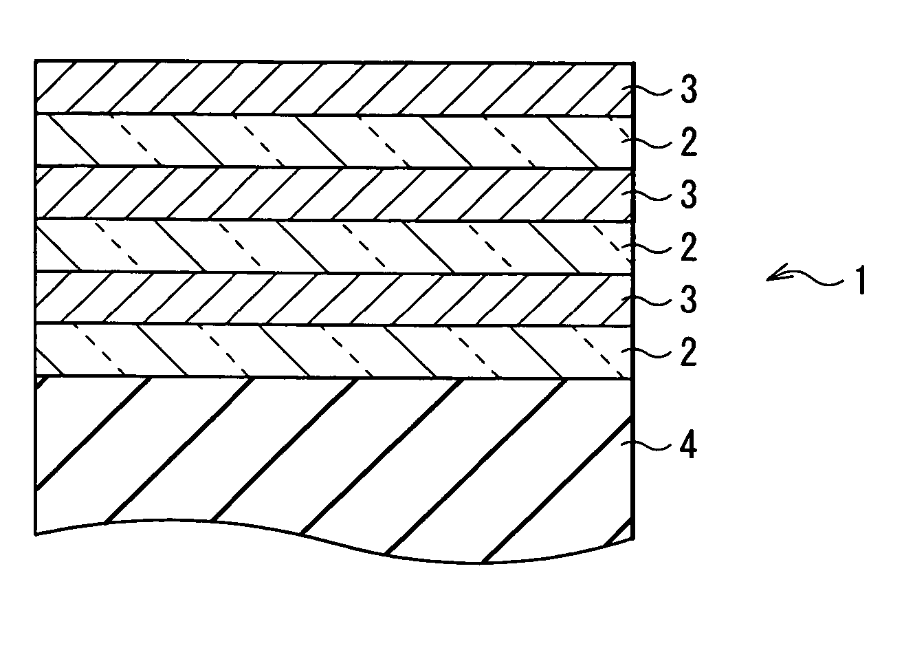
[0073] First, a Si wafer on which a 500-nm thick SiO2 film was formed was used as a substrate. Next, a magnetic thin film for high frequencies was deposited on the substrate by use of a facing target sputtering apparatus according to the following ways. That is, preliminary evacuation of the interior of the facing target sputtering apparatus was carried out to 8×10⁻⁵ Pa, thereafter Ar gas was introduced into the apparatus until the pressure thereof reached 10 Pa, and then the substrate surface was subjected to sputter etching at an RF power of 100 W for 10 minutes. Subsequently, the Ar gas flow was adjusted so that the pressure might be set to 0.4 Pa, then sputtering of a Co87Zr5Nb8 target was carried out by the power of 300 W and consequently an amorphous film with Co87Zr5Nb8 composition was produced.

[0074] Subsequently, a natural-oxidation lay...

example 2

[0078] On the basis of the above described film formation technique of Example 1, a 2.3-nm thick CoZrNb layer and a 1.0-nm thick natural oxidation layer were alternately layered each in 121 times in a successive manner, and consequently a magnetic thin film (Example 2) having a total film thickness of 400 nm (242 layers in total) was formed. At this time, the volume ratio of the natural-oxidation layer to the whole multilayer film was 30%.

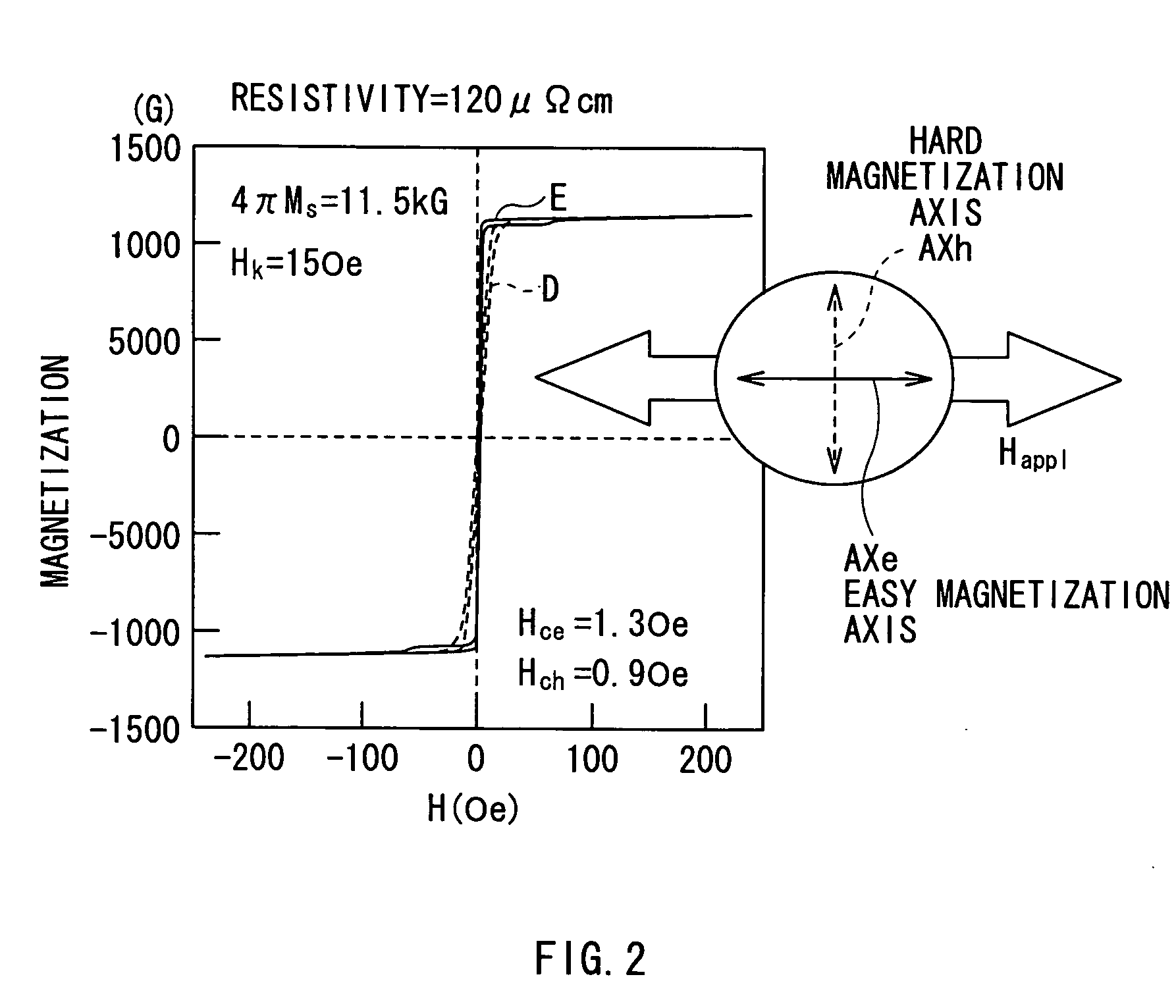
[0079] The magnetic properties of the obtained magnetic thin film are represented in Table 1. A value of saturation magnetization 4 πMs was 0.80 T (=8.0 kG), a value of coercitivity Hce in the easy magnetization direction was 1400 A / m (=17.6 Oe) and a value of coercitivity Hch in the hard magnetization direction was 2950 A / m (=37 Oe). A value of high frequency permeability property obtained was 40 at 1.0 GHz, as a value of the permeability real part (μ1), and a value of resistivity was 860 μΩcm.

example 3

[0080] Based on the film formation technique of the above-mentioned Example 1, after forming a CoZrNb layer of 1.6 nm in thickness, a 1.3 nm natural-oxidation layer was formed by introducing O2 gas with 5 sccm into the interior of the sputtering apparatus for 30 seconds to oxidize the surface of metal layers. The CoZrNb layer of 1.6 nm in thickness and the natural-oxidation layer of 1.3 nm in thickness were alternately formed 138 times respectively in a successive manner, and consequently a magnetic thin film (Example 3) having a total film thickness of 400 nm (276 layers in total) was formed. At this time, the volume ratio of the natural-oxidation layer to that of the whole multilayer film was 45%.

[0081] The magnetic properties of the obtained magnetic thin film are shown in Table 1. A value of saturation magnetization was 0.63 T (=6.3 kG), a value of coercitivity Hce in the easy magnetization direction was 1750 A / m (=22 Oe), and a value of coercitivity Hch in the hard magnetizati...


PUM

PropertyMeasurementUnit
ferromagnetic resonance frequencyaaaaaaaaaa
thicknessaaaaaaaaaa
thicknessaaaaaaaaaa

Abstract

A multilayer film (1) is formed by alternately layering a Co-based amorphous alloy layer (2) and a natural-oxidation layer (3) of the Co-based amorphous alloy (2) on a substrate (4). A magnetic thin film for high frequencies and a magnetic device which can be used in high frequency regions of the GHz band are obtained by making a volume ratio of the natural-oxidation layer (3) to the whole multilayer film (1) fall within a range of 5 to 50%. A magnetic thin film for high frequencies is also obtainable by forming a multilayer film (1) by alternately layering the Co-based amorphous alloy layer (2) having such a characteristic that a direction of magnetic field applied in a film formation process comes to be a direction of an easy magnetization axis of the Co-based amorphous alloy layer and a natural-oxidation layer (3) of the Co-based amorphous alloy, so that the easy magnetization axis of thus formed multilayer film (1) may be perpendicular to the direction of magnetic field applied in the film formation process of the multilayer film (1).

Description

TECHNICAL FIELD [0001] The present invention relates to a magnetic thin film for high frequencies used in a high frequency region of the GHz band, a method of manufacturing the same, and a magnetic device including the magnetic thin film for high frequencies, and more specifically relates to a magnetic thin film for high frequencies and a method of manufacturing the same, and a magnetic device preferably used in high frequency planar magnetic devices such as a thin film inductor and a thin film transformer and so on and in monolithic microwave integrated circuits (hereinafter referred to as “MMIC”). BACKGROUND ART [0002] In accordance with increasing demands for a miniaturization and sophistication of magnetic devices in recent years, magnetic thin film materials exhibiting a high permeability in the GHz band are in demand. [0003] For example, a MMIC, for which demand is growing for use in wireless transmitters / receivers and portable digital assistants, is a high frequency integrate...

Claims


Application Information

Patent Timeline
Patent Type & Authority Applications(United States)
IPC IPC(8): B32B15/00B32B19/00B05D5/12H01F10/16H01F10/13H01F17/00H01F41/04
CPCB82Y25/00B82Y40/00H01F10/132H01F17/0013H01F10/3286H01F41/303H01F2017/0066Y10T428/325Y10T428/32H01F41/046H01F10/12H01F10/13H01F17/00H01F41/14
Inventor CHOI, KYUNG-KUMURASE, TAKU
Owner TDK CORPARATION
Why Eureka
Try Eureka