Apparatus for and method of biasing a transistor

a transistor and apparatus technology, applied in the field of apparatus for and method of biasing transistors, can solve the problems of non-linearity of transistors, generation of harmonic components, transmissions outside of nominal transmission frequency bands having power levels, etc., to save power, reduce power requirements of circuits, and simplify the construction of analog measurement circuits

Active Publication Date: 2007-09-13
MEDIATEK INC
View PDF3 Cites 2 Cited by
  • Summary
  • Abstract
  • Description
  • Claims
  • Application Information

AI Technical Summary

Benefits of technology

[0042] It is thus possible to provide an apparatus for setting the bias conditions for a transistor to a point to optimise a characteristic of that transistor, such as a given order non-linearity, whilst simultaneously simplifying the construction of the analog measurement circuit required to determine the bias point and also reducing the power requirements of the circuit by enabling the analog portion to be shut down to save power once the bias measurement has been made.
[0043] In a preferred embodiment the apparatus is arranged to search for a biasing point to substantially reduce the 3rd order derivative to zero, or to a minimum magnitude. In this embodiment the test circuit is arranged to estimate the second order derivative for the value of the bias being provided by the bias circuit. This requires only three transistors biased at slightly different voltages within the test circuit and furthermore the current ratio between the most current carried by a transistor and the least current is only 2:1. This means that the performance of this analog test circuit may be far more reliable than, say, the third order circuit shown in the prior art, as the opportunities for mismatch are reduced.
[0044] Additionally the test circuit only need to be powered up when the controller wishes to check the bias voltage. This gives rise to significantly reduced power consumption.

Problems solved by technology

However, in reality, transistors exhibit non-linearities in their transfer characteristic and this can give rise to the generation of harmonic components, even when amplifying an AC signal having a monotonic frequency F1.
Non-linearities in amplifiers or mixers may result in transmissions outside of a nominal transmission frequency band having power levels in excess of those permitted by the licensing authorities.
Similarly, the generation of harmonic signals or mixing of signals (such as inter-modulating of interfering signals) within a receiver due to non-linearities could degrade reception of a desired signal.
Then after VGS is reached a square law like behaviour is found, but as the voltage increases this behaviour starts to fail as the field related effects become more significant.
Unfortunately, it can also be seen that the gradient of the line shown in FIG. 3c is very steep around this zero intercept point and hence any deviation away from the ideal position quickly introduces a significant amount of third order non-linearity.
Furthermore, if the characteristics of the circuit vary from circuit to integrated circuit within the same batch and from wafer to wafer within different batches it is not sufficient or desirable merely to set up the same bias voltage for all instances of this circuit because only a very small proportion of them are likely to be biased anywhere near the correct bias conditions and a large proportion of the circuits are biased at a point where they give rise to quite pronounced third order non-linearities.
In practical terms it would be very time consuming to characterise each instance of an amplifier that was fabricated, especially as the bias point may change with temperature and age.
It is possible to scale the transistors used an the currents that they pass so as to reduce the current drawn, but this reduces the matching between the amplifier and the derivative calculating circuit.
Any mismatch will give rise to an error in the result.
It is suspected that whilst this circuit looks good in theory there will be a trade off between matching and power consumption which may make implementation difficult in system having a tight power budget.

Method used


Image

  • Apparatus for and method of biasing a transistor
  • Apparatus for and method of biasing a transistor
  • Apparatus for and method of biasing a transistor

Examples


Embodiment Construction

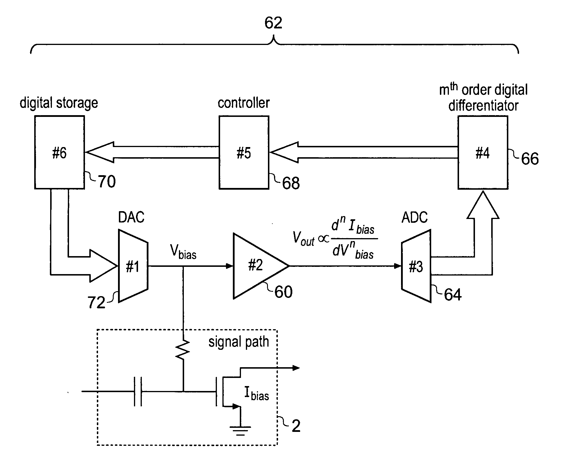
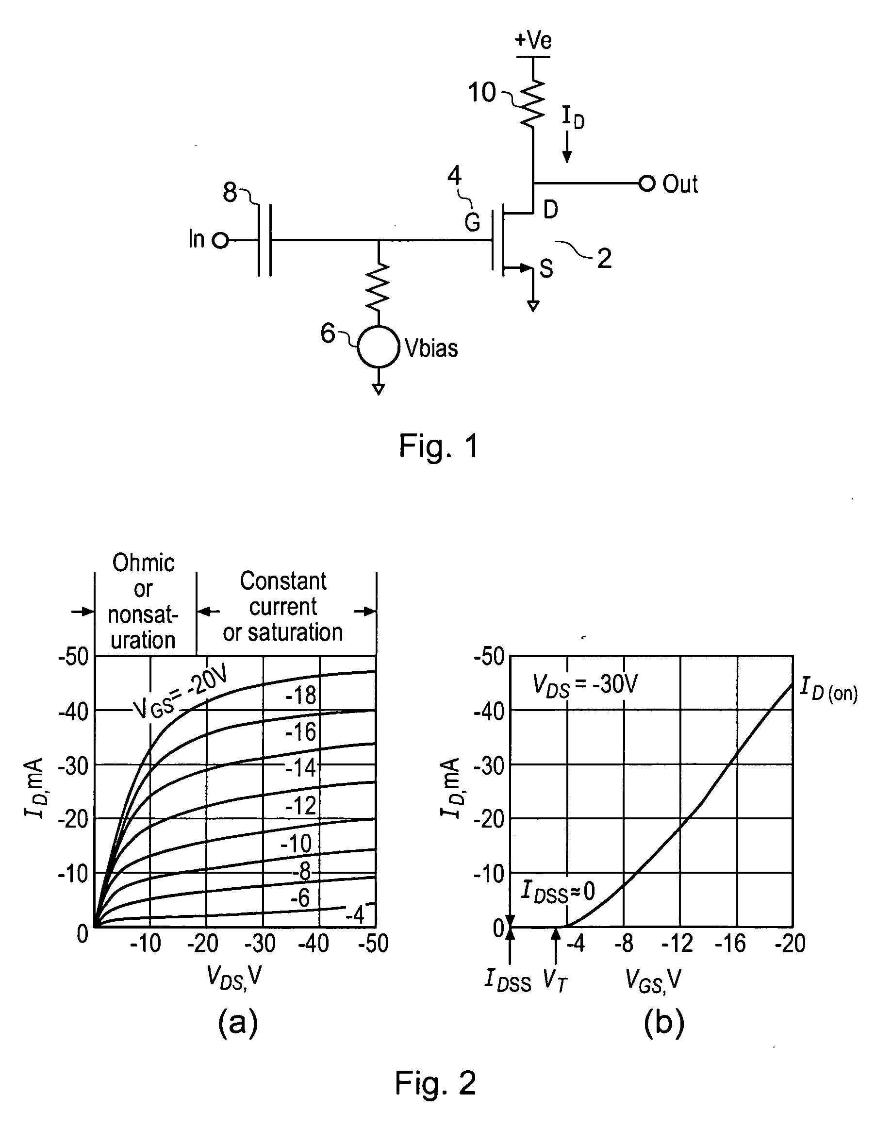
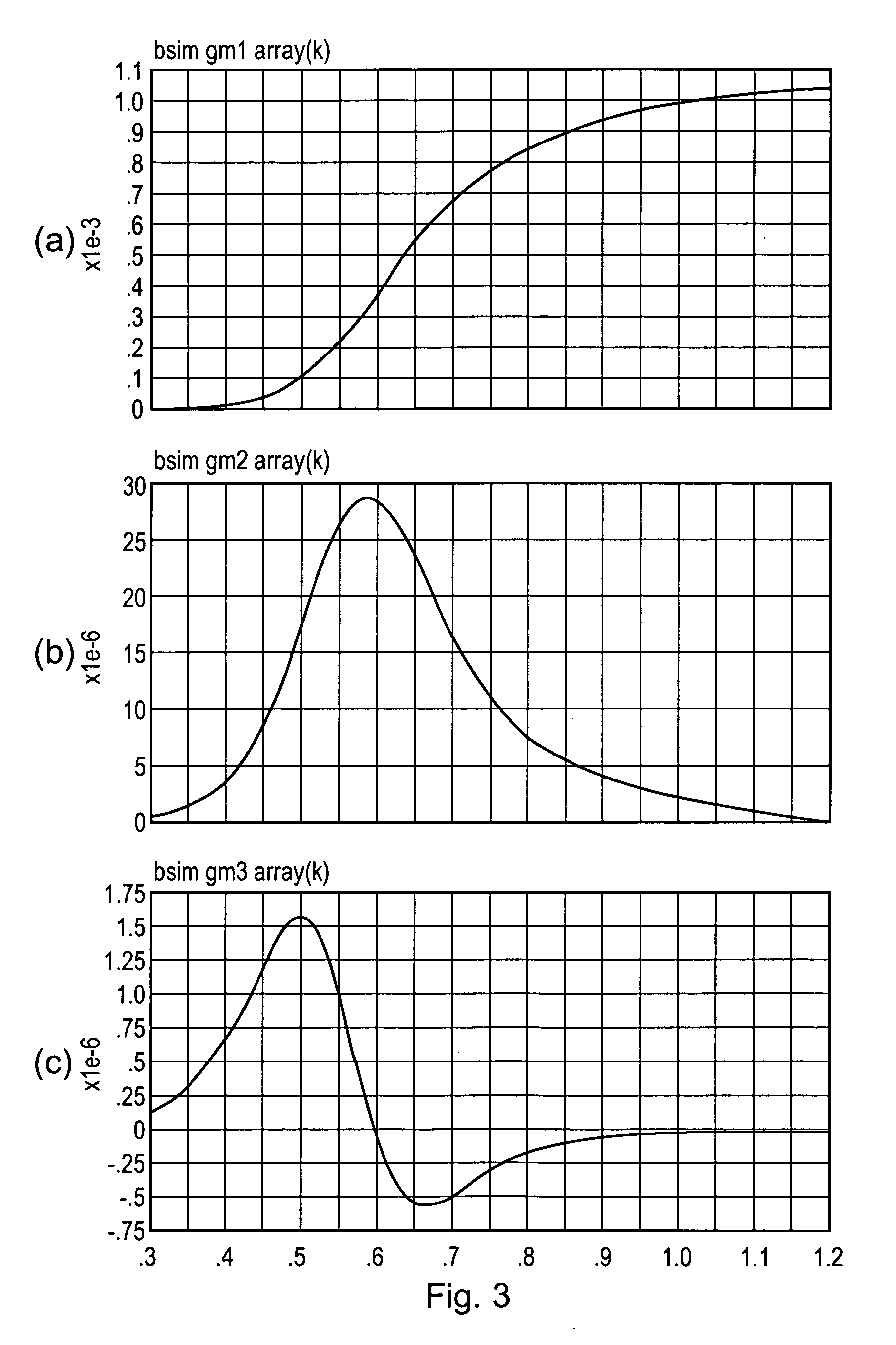
[0064]FIG. 6 schematically illustrates an embodiment of the present invention which is arranged to provide a bias voltage for the transistor amplifier 2. Given that the amplifier 2 will be in use a test circuit 60 is provided which models or replicates an aspect of the performance of the amplifier 2. Therefore, if it is desired to minimise the third harmonic distortion by biasing the transistor to the point where a third derivative, i.e. Gm3, is zero then the test circuit 60 may be fabricated to mirror the transistor amplifier circuit itself or may include a derivative calculating circuit adapted to form a derivative lower than the third order, for example the first order or second derivative. An example of a circuit for calculating a second order derivative is shown in FIG. 7 and will be discussed more fully later.

[0065] An output of the test circuit is provided as an analog input to a digital control system, generally designated 62, and comprising an analog to digital converter 6...


PUM


Abstract

An apparatus for biasing a transistor, comprising: a controllable bias generator; a test circuit; a digital Mth order differentiator responsive to an output of the test circuit; and a controller responsive to the digital Mth order differentiator for controlling the controllable bias generator; wherein the test circuit is configured to calculate an Lth order derivative of the transistor's performance.

Description

FIELD OF THE INVENTION [0001] The present invention relates to an apparatus for, and a method of, biasing a transistor at a bias point so as to reduce a selected non-linearity within the transistor. BACKGROUND TO THE INVENTION [0002] It is well known to use transistors within mixers and amplifiers. If the transistor was perfectly linear, such that, for example, current flowing through the transistor was linearly proportional to a voltage at the gate of the transistor where the transistor is a field effect transistor, or was proportional to the voltage at the base of the transistor, where the transistor is a bi-polar transistor, then high performance amplifier design would be much simplified. However, in reality, transistors exhibit non-linearities in their transfer characteristic and this can give rise to the generation of harmonic components, even when amplifying an AC signal having a monotonic frequency F1. [0003] The reduction or elimination of harmonics is particularly important...

Claims


Application Information

Patent Timeline
Patent Type & Authority Applications(United States)
IPC IPC(8): H03F3/04
CPCH03F1/0211H03F1/0261H03F1/223H03F1/301H03F2200/453H03F2200/18H03F2200/321H03F2200/447H03F1/3205
Inventor STRANGE, JONATHAN RICHARD
Owner MEDIATEK INC
Why Eureka
Try Eureka