Method for producing an organic thin film transistor and an organic thin film transistor produced by the method

Inactive Publication Date: 2007-09-13
FLEX DISPLAY SOLUTIONS LLC
View PDF17 Cites 49 Cited by
  • Summary
  • Abstract
  • Description
  • Claims
  • Application Information

AI Technical Summary

Benefits of technology

[0017] The dropping process for forming the organic semiconductor layer may be an ink jet process. In the ink jet process, dropping is easy to control, and the volume of the organic semiconductor material to be dropped can be regulated.
[0018] Thus, the organic semiconductor layer can be formed by applying one drop of an organic semiconductor material by an ink jet process, and the organic semi

Problems solved by technology

As the number of drops is increasing, the time for dropping becomes longer, which causes a problem that the productivity becomes lower.
Also, a semiconductor lay

Method used


Image

  • Method for producing an organic thin film transistor and an organic thin film transistor produced by the method
  • Method for producing an organic thin film transistor and an organic thin film transistor produced by the method
  • Method for producing an organic thin film transistor and an organic thin film transistor produced by the method

Examples


Example

EXAMPLE 1

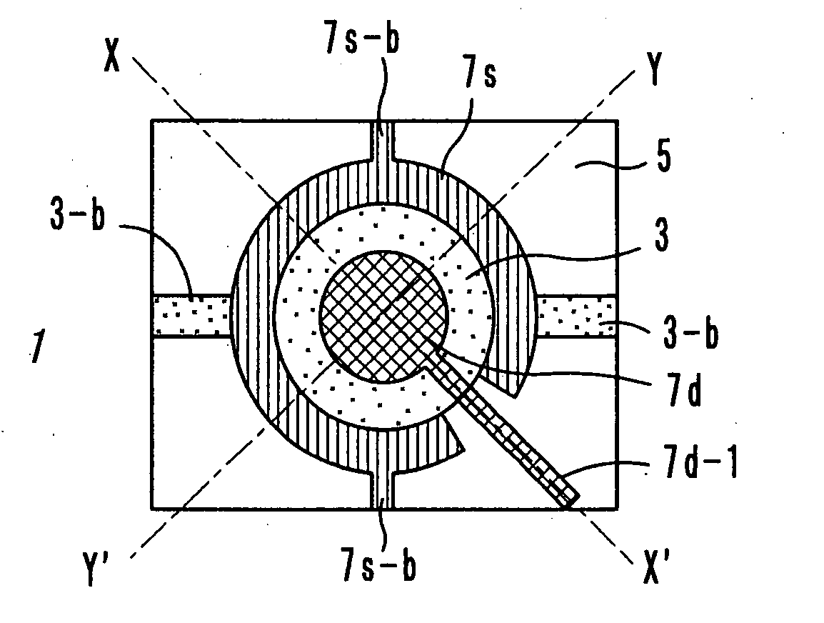
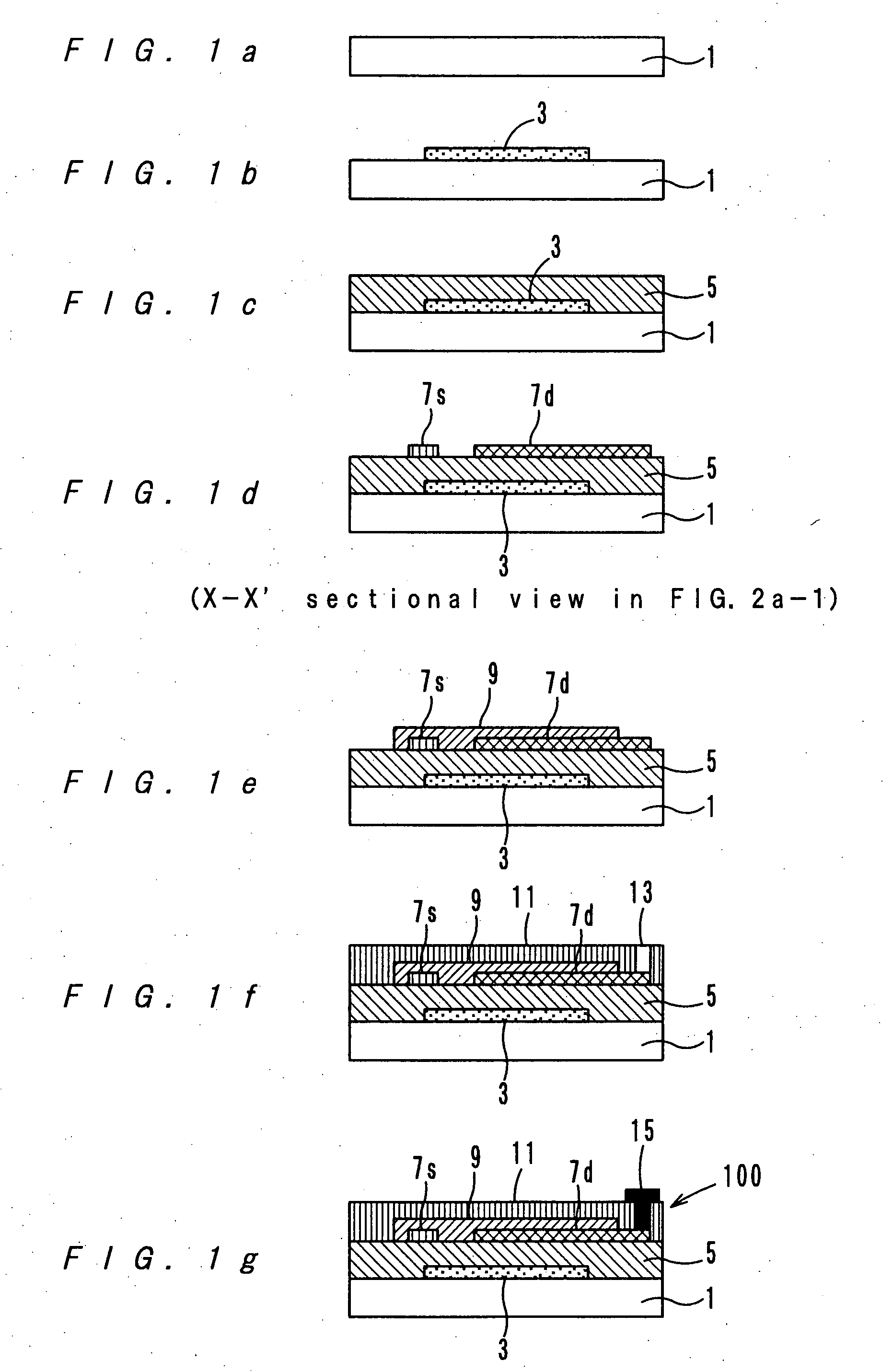
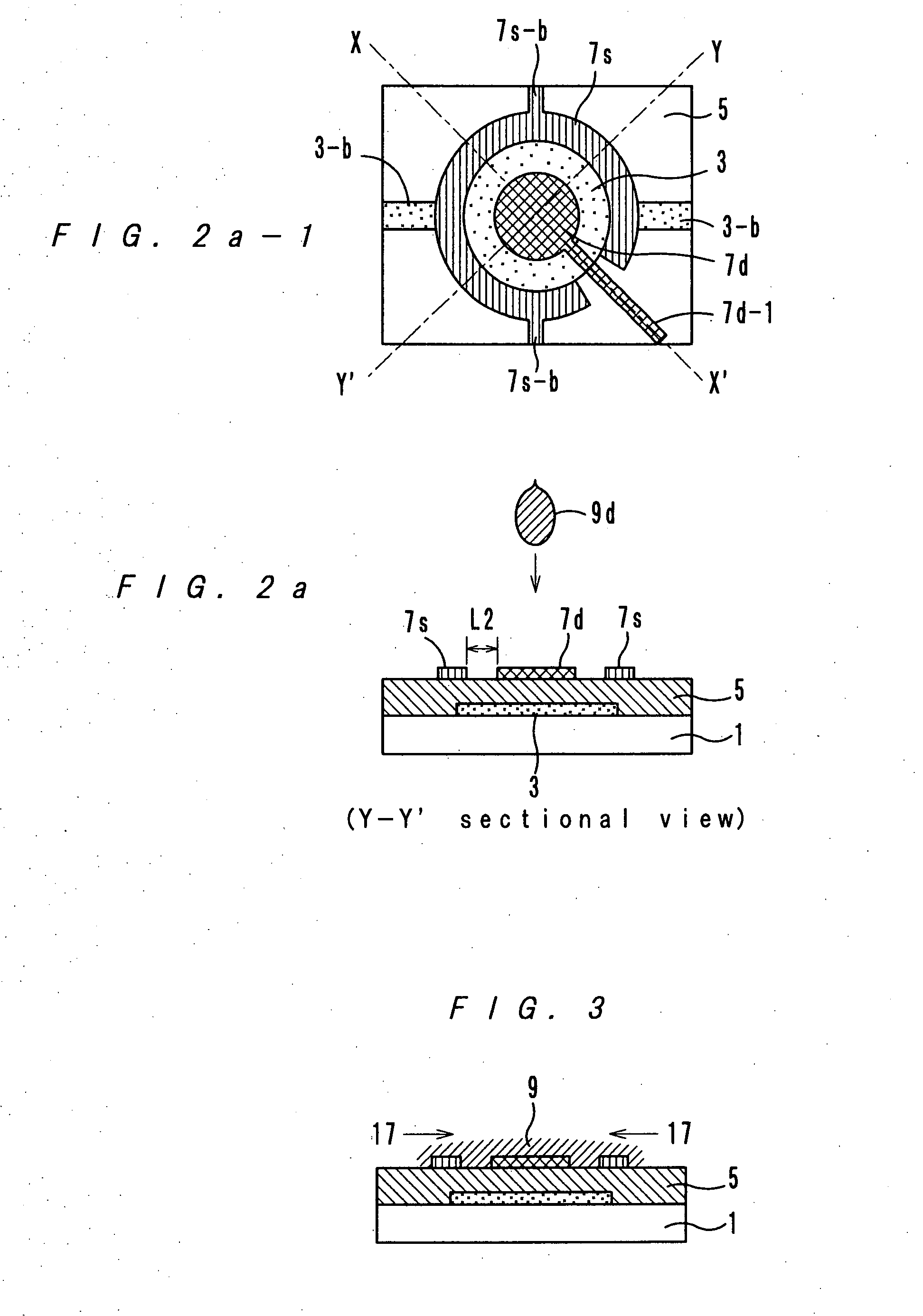
[0080] As a first example, an OFTF 100 of a bottom gate bottom contact type as shown by FIG. 1 was produced. The production processes are described referring to FIGS. 1a-1g.

[0081] On a glass substrate 1 shown by FIG. 1a, a kind of aluminum alloy, namely, aluminum-neodymium (AlNd), was formed into a film with a thickness of 150 nm by sputtering. Then, photolithography and etching were performed toward the AlNd film, and thereby, a circular gate electrode 3 was formed (see FIG. 1b).

[0082] Next, as a gate insulating film 5, SiO2 was formed into a film with a thickness of 300 nm by a plasma CVD process (see FIG. 1c).

[0083] Next, a resist pattern was formed by photolithography and etching so that a source electrode 7s which is a fragmental circle with a center hole and a drain electrode 7d which is in concentric with the source electrode 7s and which has a leading line 7d-1 could be formed by a lift-off method.

[0084] Next, a chromium film with a thickness of 5 nm was formed...

Example

EXAMPLE 2

[0097] As a second example, an OTFT 400 of a bottom gate bottom contact type was produced. The OTFT 400 was produced through the same processes as the OTFT 100 of the example 1. The differences from the OTFT 100 were that the OTFT 400 shown by FIG. 4a-1, had a circular source electrode 7s with a center hole and a circular drain electrode 7d and that the OTFT 400 had a contact hole 13 above the drain electrode 7d to connect the drain electrode 7d to a pixel electrode.

[0098]FIG. 4a shows a state wherein after forming a gate electrode 3 on a glass substrate 1, a gate insulating film 5 was formed, and further the source electrode 7s and the drain electrode 7d were formed on the gate insulating film 5. FIG. 4a is a sectional view taken along the line X-X′ in FIG. 4a-1.

[0099]FIG. 4b shows a state wherein after forming the source electrode 7s and the drain electrode 7d, an organic semiconductor layer 9 was formed.

[0100]FIG. 4c shows a state wherein after forming the organic se...

Example

EXAMPLE 3

[0102] As a third example, an OTFT 500 of a bottom gate bottom contact type was produced. As FIGS. 5a-1 and 5a-5c show, in order to form a contact hole 13 in the OTFT 500, a water repellent layer was formed on a drain electrode.

[0103] On a glass substrate 1, a kind of an aluminum alloy, namely, aluminum-neodymium (AlNd) was formed into a film with a thickness of 150 nm by sputtering. Then, photolithography and etching were performed toward the AlNd film, and thereby, a circular gate electrode 3 was formed.

[0104] Next, as a gate insulating film 5, SiO2 was formed into a film with a thickness of 300 nm by a plasma CVD process.

[0105] Next, as shown by FIG. 5a-1, a resist pattern was formed by photolithography and etching so that a circular source electrode 7s with a center hole and a drain electrode 7d which is in concentric with the source electrode 7s could be formed by a lift-off method.

[0106] Next, a chromium film with a thickness of 5 nm was formed, and further a gol...


PUM


Abstract

A method for producing an organic thin film transistor having, on a substrate, a source electrode, a gate electrode, a drain electrode, an insulating layer and an organic semiconductor layer. The method has a step of forming the source electrode and the drain electrode such that one of the source electrode and the drain electrode which is an inner-located electrode has an outer circumference which is circular or polygonal and that the other electrode which is an outer-located electrode has an inner circumference facing the outer circumference of the inner-located electrode, the inner circumference being of a shape which is substantially concentric with the outer circumference of the inner-located electrode. The method also has a step of forming the organic semiconductor layer for connecting the source electrode and the drain electrode to each other by a process of dropping an organic semiconductor material.

Description

[0001] This application is based on Japanese Patent Application Nos. 2006-60760 and 2007-24031, the contents of which are incorporated herewith by reference. BACKGROUND OF THE INVENTION [0002] 1. Field of the Invention [0003] The present invention relates to a method for producing an organic thin film transistor and an organic thin film transistor produced by the method. [0004] 2. Description of Related Art [0005] Recently, as switching elements for driving pixels of a flat panel display device and an electronic paper, which are next-generation high-quality low-price devices, organic thin film transistors (OTFTs) draw attention. [0006] An organic thin film transistor is basically of the same structure as that of a silicon thin film transistor. However, while the silicon thin film transistor has a semiconductor active layer made of silicon, the organic thin film transistor has a semiconductor active layer made of an organic material. Such organic thin film transistors can be produced...

Claims


Application Information

Patent Timeline
IPC IPC(8): H01L51/40
CPCH01L51/0023H01L51/0055H01L51/102H01L51/0545H01L51/0525H10K71/621H10K85/623H10K10/472H10K10/82H10K10/466
Inventor YAMADA, JUNHIRAO, YUYAMASAZUMI, NAOKI
Owner FLEX DISPLAY SOLUTIONS LLC
Why Eureka
Try Eureka