Substrate processing apparatus, deposit monitoring apparatus, and deposit monitoring method

Inactive Publication Date: 2007-09-20
TOKYO ELECTRON LTD
View PDF6 Cites 25 Cited by
  • Summary
  • Abstract
  • Description
  • Claims
  • Application Information

AI Technical Summary

Benefits of technology

[0011]According to the first aspect of the present invention, the first conductor and the second conductor are disposed separated from one another, and are connected to a sensor that obtains data relating to the capacitance. If deposit, which generally has a high permittivity, becomes attached to the surface of the first conductor and the second conductor, then a capacitor having a high capacitance is formed, data relating to this capacitance, for example the value of the

Problems solved by technology

In this way, the inner wall of the chamber is fouled with deposit during the plasma processing.
If the inner wall of the chamber is severely fouled with deposit, then the distribution of plasma in the chamber is affected, and hence the reproducibility of the plasma processing worsens.
However, with such a statistical technique, to improve the accuracy of the prediction of the environment in the chamber, a large amount of data must be o

Method used


Image

  • Substrate processing apparatus, deposit monitoring apparatus, and deposit monitoring method
  • Substrate processing apparatus, deposit monitoring apparatus, and deposit monitoring method
  • Substrate processing apparatus, deposit monitoring apparatus, and deposit monitoring method

Examples


Embodiment Construction

[0040]Embodiments of the present invention will be described in detail below with reference to the drawings.

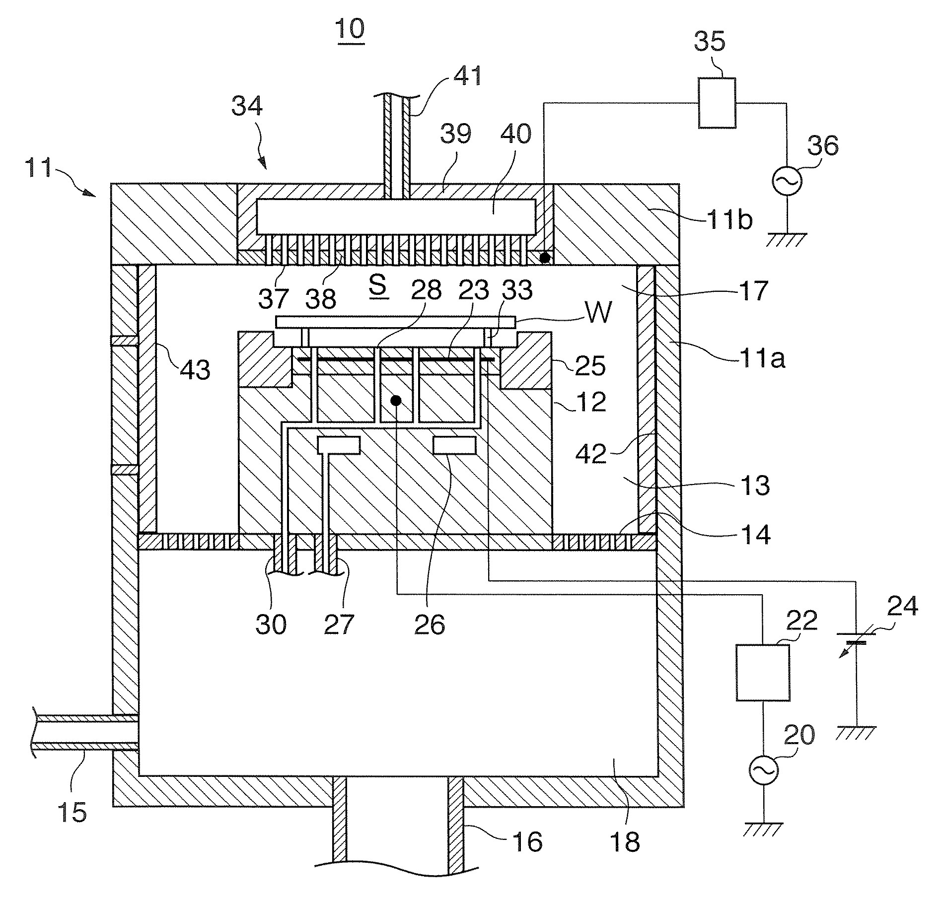
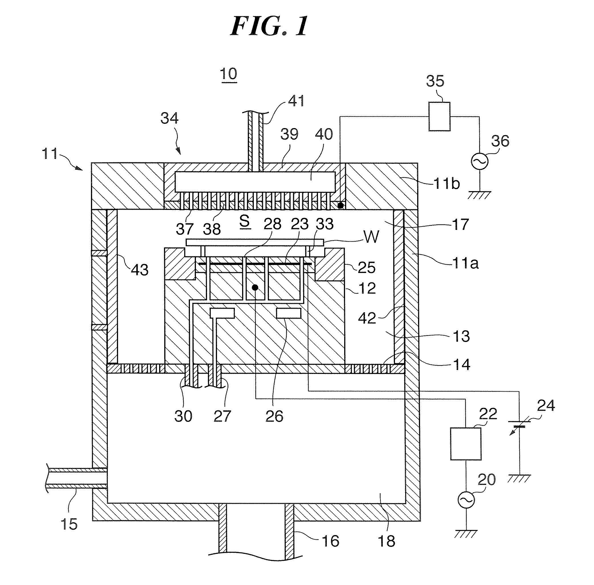
[0041]FIG. 1 is a sectional view schematically showing the construction of a substrate processing apparatus according to an embodiment of the present invention. The substrate processing apparatus is constructed such as to carry out etching processing on semiconductor wafers as substrates to be processed.

[0042]As shown in FIG. 1, the substrate processing apparatus 10 has a cylindrical chamber 11 (processing chamber) housing a semiconductor wafer (hereinafter referred to merely as a “wafer”) W having a diameter of, for example, 300 mm. A cylindrical susceptor 12 is disposed in the chamber 11 as a stage on which the wafer W is mounted.

[0043]In the substrate processing apparatus 10, a side exhaust path 13 that acts as a flow path through which gas above the susceptor 12 is exhausted out of the chamber 11 is formed between an inner wall 11a of the chamber 11 and a side face of the ...


PUM

PropertyMeasurementUnit
Dielectric polarization enthalpyaaaaaaaaaa
Frequencyaaaaaaaaaa
Fouling propertiesaaaaaaaaaa

Abstract

A substrate processing apparatus enable fouling due to deposit to be monitored in real time. To monitor deposit attached to an inner wall surface of a processing chamber in which processing is carried out on a substrate, a deposit monitoring apparatus of the substrate processing apparatus includes a sensor for measuring a capacitance between two conductors spaced apart from each other and both connected to the sensor. The capacitance between the conductors increases with increase in an mount of deposit and reflects the state of fouling due to deposit.

Description

BACKGROUND OF THE INVENTION[0001]1. Field of the Invention[0002]The present invention relates to a substrate processing apparatus, a deposit monitoring apparatus, and a deposit monitoring method, and in particular relates to a substrate processing apparatus that enables monitoring of deposit attached to an inner wall surface of a processing chamber (chamber) in which predetermined processing is carried out on substrates to be processed.[0003]2. Description of the Related Art[0004]In plasma processing for manufacturing semiconductor chips, etching of a thin film formed on a semiconductor wafer (hereinafter referred to merely as “wafer”) as a substrate to be processed, or CVD (chemical vapor deposition) in which a predetermined material is deposited on the wafer so as to form a thin film, is carried out in a chamber housing the wafer.[0005]CVD is a process in which a thin film of a predetermined material is formed on a wafer, and hence a deposit of the predetermined material inevitabl...

Claims


Application Information

Patent Timeline
IPC IPC(8): C23C14/54B05C11/00
CPCH01L21/67253C23C16/4401H01L22/00
Inventor YAMAZAWA, YOHEI
Owner TOKYO ELECTRON LTD
Why Eureka
Try Eureka