Eureka AIR delivers breakthrough ideas for toughest innovation challenges, trusted by R&D personnel around the world.

Piezoresistance element and semiconductor device having the same

Inactive Publication Date: 2007-09-20
LAPIS SEMICON CO LTD
View PDF4 Cites 15 Cited by
  • Summary
  • Abstract
  • Description
  • Claims
  • Application Information

AI Technical Summary

Benefits of technology

[0012]Accordingly, a first object of the present invention is to provide a piezoresistance element, in which a resistance value thereof is hardly changed due to an external electric field.
[0013]A second object of the present invention is to provide a piezoresistance element, which has a high breakdown voltage and a less amount of leak current.
[0014]A third object of the present invention is to provide a piezoresistance element, which has improved mechanical strength, a longer vibration lifetime and higher product reliability.

Problems solved by technology

However, according to the above-describe method or technique (1), the resistance layer is located at an upper surface of the semiconductor substrate, so that a resistive value of the resistance layer may be changed undesirably due to external electric field (surface-electric-field effect).
As a result, noises are increased due to leak current.
Such a crystal defect could be recovered in a following thermal treatment to some extent, but could not be recovered completely.
A defect due to a fabrication process may decrease or weaken mechanical strength of beams, on which piezoresistance elements are formed.
Further, a vibrational lifetime of the sensor may be shortened, and product reliability may be decreased.

Method used


Image

  • Piezoresistance element and semiconductor device having the same
  • Piezoresistance element and semiconductor device having the same
  • Piezoresistance element and semiconductor device having the same

Examples


Embodiment Construction

[0049]In the following detailed description of the preferred embodiments, reference is made to the accompanying drawings which form a part hereof, and in which is shown by way of illustration specific preferred embodiments in which the inventions may be practiced. These preferred embodiments are described in sufficient detail to enable those skilled in the art to practice the invention, and it is to be understood that other preferred embodiments may be utilized and that logical, mechanical and electrical changes may be made without departing from the spirit and scope of the present inventions. The following detailed description is, therefore, not to be taken in a limiting sense, and scope of the present inventions is defined only by the appended claims.

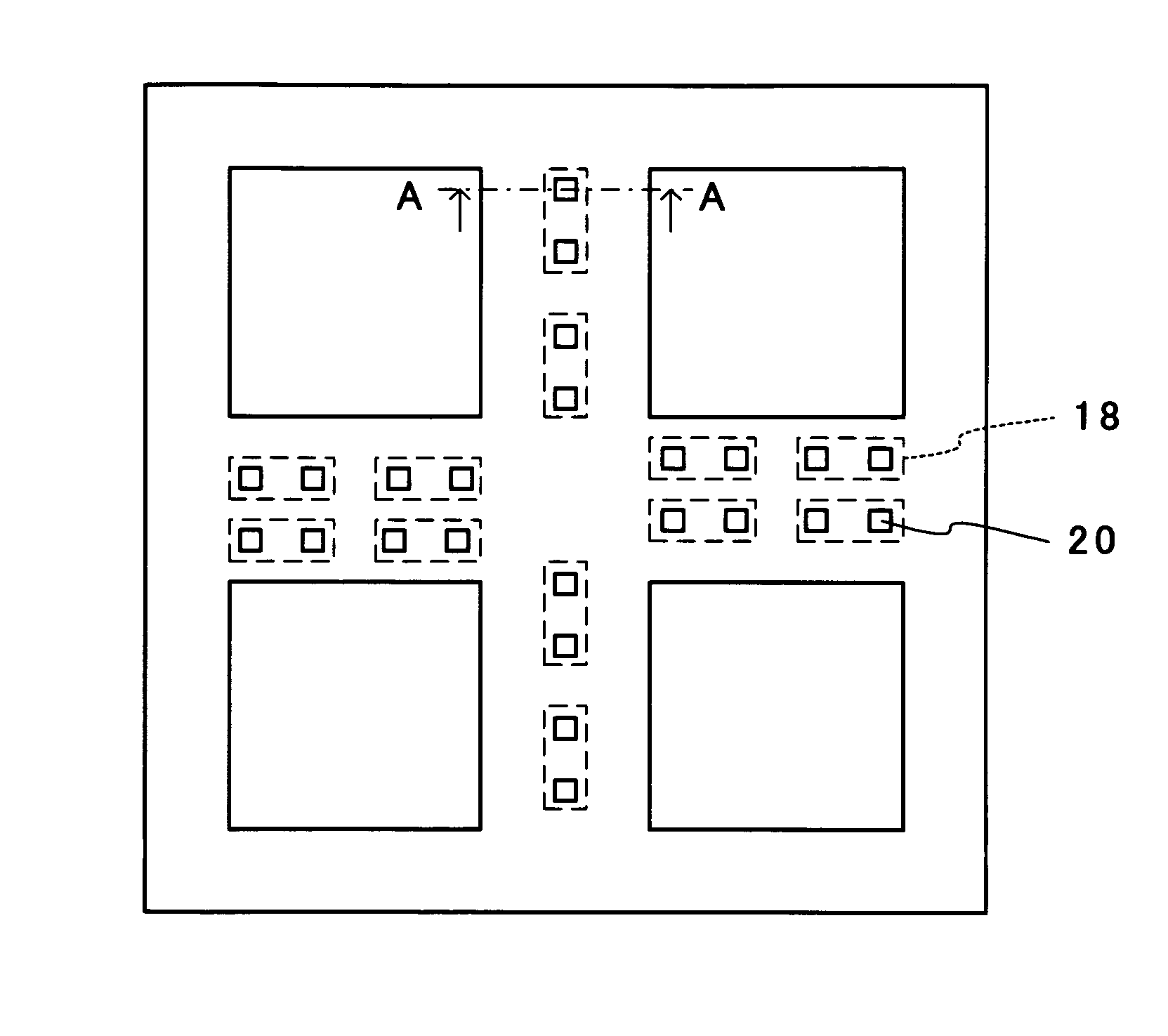
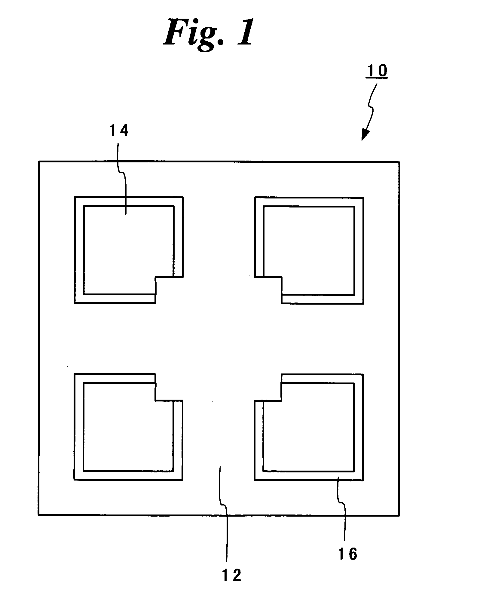
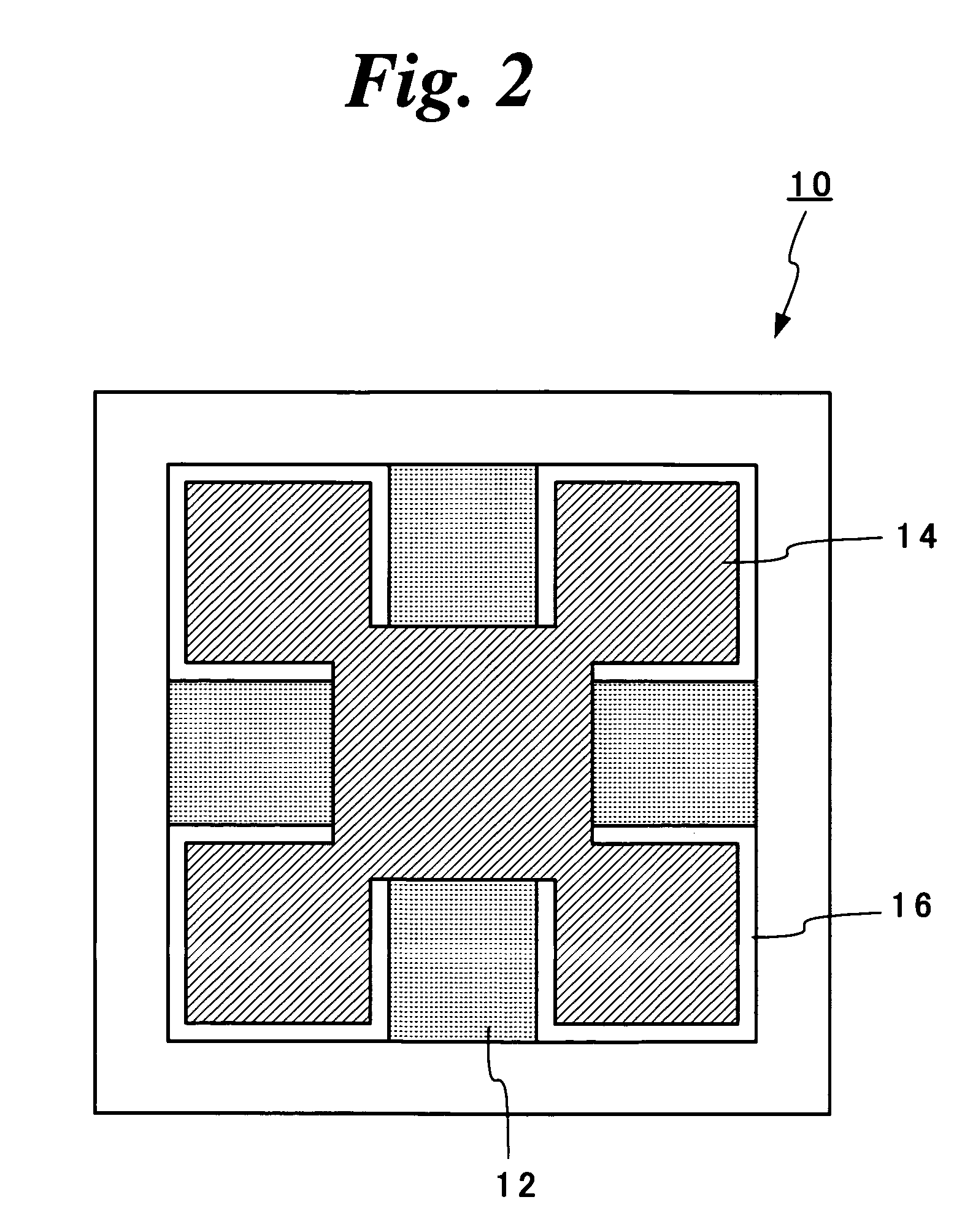
[0050]Now, preferred embodiments of the present invention will be described referring to the attached drawings. FIG. 1 is a plane view illustrating a summarized structure of an acceleration sensor (semiconductor device) according to a...


PUM


Abstract

A piezoresistance element formed in a semiconductor substrate, includes a pair of contact regions formed in the semiconductor substrate; a groove formed between the pair of contact regions; a resistance layer formed in the groove, the resistance layer having a conductive type opposing to the semiconductor substrate; and a silicon layer formed on the resistance layer, the silicon layer having a conductive type corresponding to the semiconductor substrate.

Description

CROSS REFERENCE TO RELATED APPLICATION[0001]This application claims the priority of application No. 2006-72750, filed on May 16, 2006 in Japan, the subject matter of which is incorporated herein by reference.TECHNICAL FIELD OF THE INVENTION[0002]This invention relates to a structure of a piezoresistance element and a semiconductor device having the same.BACKGROUND OF THE INVENTION[0003]In recent years, a micro structure, which is a small in sized of hundreds micron meters, has been an object of public attention in the semiconductor manufacturing field. Such a micro structure is fabricated using a micro-machine technology, which is an application of semiconductor fine processing technology. A micro structure has been considered to be applied to a high-frequency device, including sensors and optical switches for optical communication. In general, a microstructure based on a micro-machine technology is fabricated using a semiconductor process, so that such a device can be integrated on...

Claims


Application Information

Patent Timeline
IPC IPC(8): H01L29/82H01L29/84
CPCG01P15/0802H01L29/84G01P15/18G01P15/123G01P2015/0842E02D17/04E02D17/083E02D2200/115E02D2200/1671E02D2600/20
Inventor IKEGAMI, NAOKATSU
Owner LAPIS SEMICON CO LTD
Why Eureka
Eureka Blog
Learn More