Integrated passive device substrates

a passive device and substrate technology, applied in the direction of capacitors, semiconductor/solid-state device details, inductances, etc., can solve the problems of reducing the performance of capacitors, reducing the density of stable charge carrier traps, and reducing the efficiency of capacitors

Inactive Publication Date: 2007-09-20
SYCHIP
View PDF6 Cites 11 Cited by
  • Summary
  • Abstract
  • Description
  • Claims
  • Application Information

AI Technical Summary

Benefits of technology

[0012] We have developed an improved IPD substrate that addresses problems with accumulation of mobile charge carriers at or near the surface of an IPD substrate. The improved substrate has a layer of polysilicon added between the intrinsic silicon substrate and the surface oxide. As known in the art, typical silicon substrates are at least lightly doped. In terms of commercially available silicon material, a standard silicon wafer will have a resistivity of approximately 5-30 ohm cm. Reference to intrinsic silicon material in connection with this invention is intended to mean silicon having a resistivity higher than 500 ohm cm, and preferably higher than 1000 ohm cm. Resistivity values of 4000 ohm cm or higher are also contemplated. The surface oxide is preferably silicon dioxide, but other oxides may be used, such as tantalum oxide, titanium oxide, etc. The polysilicon layer contains a high density of stable charge carrier traps due to the large number of crystal defects in the polysilicon layer. Charge that accumulates at the Si / SiO2 interface is converted from mobile charge to fixed charge by these traps.

Problems solved by technology

But, more fundamentally, the size of many passive devices is a function of the frequency of the device, and thus is inherently relatively large.
However, still, there is unrelenting pressure to produce more compact and area efficient IPDs.
When the surface mounted IPD device is a capacitor for example, the MOS structure acts as an added series capacitor, and degrades the capacitor performance.
Moreover, if the accumulated charge renders the substrate semiconducting, the performance of all of the IPD components on the surface is impaired due to the reduced resistivity of the entire substrate.
A significant part of these adverse effects on passive components in the IPD device is due to the fact that much of the accumulated charge just described is mobile.
Due to the mobility of the accumulated charge, the adverse electric field effects from the accumulated charge varies with applied voltage.
It is well known that ion implantation damage reduces charge mobility in silicon due to the creation of crystal damage and the production of charge trapping sites.

Method used


Image

  • Integrated passive device substrates
  • Integrated passive device substrates
  • Integrated passive device substrates

Examples


Embodiment Construction

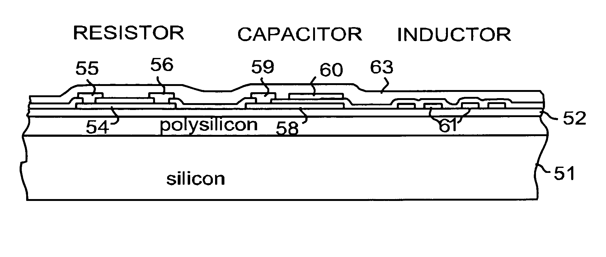
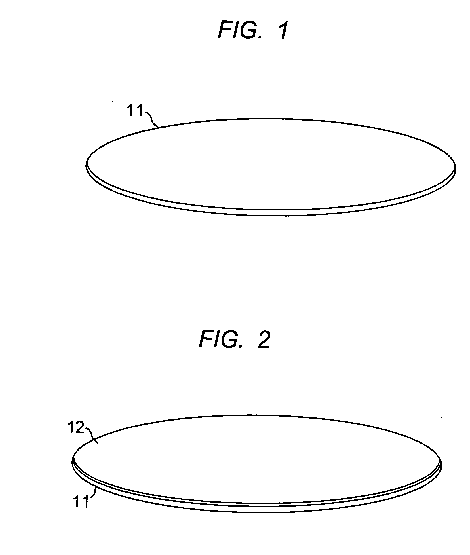
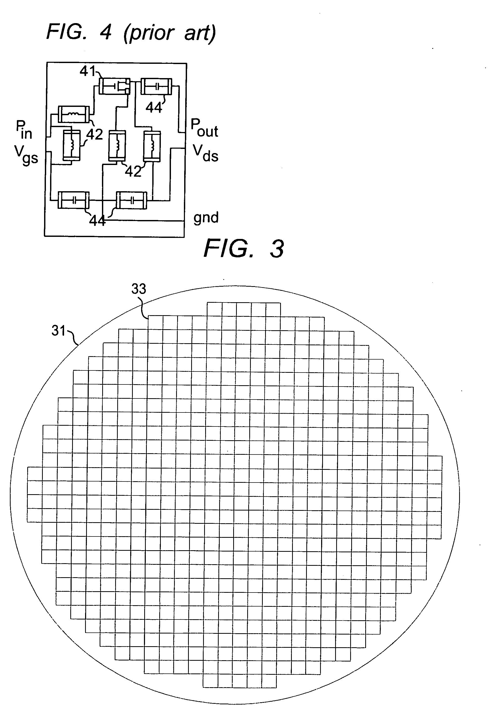
[0020]FIG. 1 is a view of a silicon wafer 11. The substrate wafer is a single crystal silicon wafer cut from a boule, and has properties described earlier, in particular, intrinsic resistivity. In this description, reference to silicon means single crystal silicon. Silicon wafers are produced in many sizes, but typically the larger the diameter of the wafer, the lower the potential device cost. Currently, silicon wafers are available in diameters up to twelve inches. With twelve inch wafers state of the art, that size will be used as the example in the following description. It should be understood that smaller wafers, for example 6″ or 8″, are also useful. The single crystal wafer has useful attributes for an IPD substrate wafer. It is typically thin (e.g. 200-700 microns), but is robust physically, and can be handled and processed. It is very flat over a large area. It has a highly polished uniformly smooth surface. And it is compatible with silicon wafer fabrication processes and...


PUM


Abstract

The specification describes an integrated passive device (IPD) that is formed on a silicon substrate covered with an oxide layer. Unwanted accumulated charge at the silicon/oxide interface are rendered immobile by creating trapping centers in the silicon surface. The trapping centers are produced by a polysilicon layer interposed between the silicon substrate and the oxide layer.

Description

FIELD OF THE INVENTION [0001] This invention relates to integrated passive devices (IPDs) and more specifically to IPDs formed on silicon substrates. BACKGROUND OF THE INVENTION [0002] (Portions of the technical material contained in this section may not be prior art.) [0003] State of the art radio frequency (RF) electrical circuits use large quantities of passive devices. Many of these circuits are used in hand held wireless products. Accordingly, miniaturization of passive devices and passive device circuits is an important goal in RF device technology. [0004] Integration and miniaturization of passive devices on the scale of active silicon devices has not occurred for at least two reasons. One, typical passive devices to date employ different material technologies. But, more fundamentally, the size of many passive devices is a function of the frequency of the device, and thus is inherently relatively large. However, still, there is unrelenting pressure to produce more compact and...

Claims


Application Information

Patent Timeline
Patent Type & Authority Applications(United States)
IPC IPC(8): H01L29/00H01L21/20
CPCH01L21/84H01L23/66H01L27/016H01L27/13H01L28/10H01L28/20H01L28/40H01L2924/13091H01L2224/16H01L2924/19011H01L2924/19103H01L2924/00H01L2224/05572H01L2224/05573H01L2924/00014H01L2224/05599
Inventor DEGANI, YINONFAN, YUGAO, CHARLEY CHUNLEILAU, MAUREENSUN, KUNQUANSUN, LIGUO
Owner SYCHIP
Why Eureka
Try Eureka