
Eureka
For R&D, Eureka makes reading and utilizing patents & technical documents easy.
Eureka AIR
Designed for self-driven R&D workflows. Generate viable solutions, solve complex R&D challenges, empower your innovation with AI.

Eureka Materials
Designed for material experts only. Revolutionize your material R&D, from search, analyze, to developing new materials.

TechResearch
Generate reliable direction feasibility study reports for your R&D in just a few steps.

TechSeek
Discover and master advanced knowledge NOW. Basics, ideas, possibilities, all at once.

TechMind
As an expert in R&D Theories, TechMind can generates customized viable solutions instantly.

TechRisk
Analyze your overall solution with one click, know your potential R&D risks in advance.

TechMonitor
Get weekly tech updates, stay abreast of the latest tech innovations and key insights.
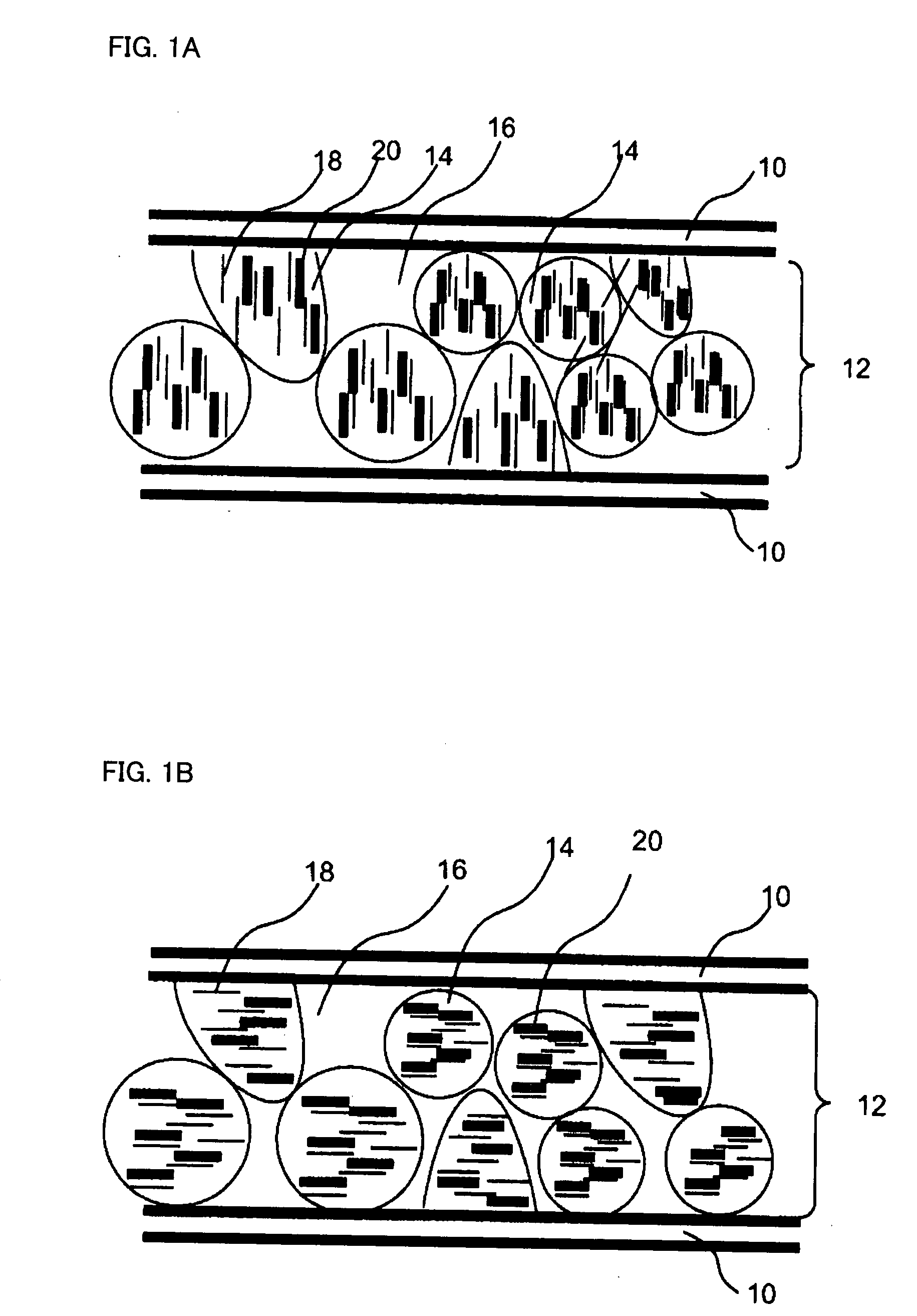
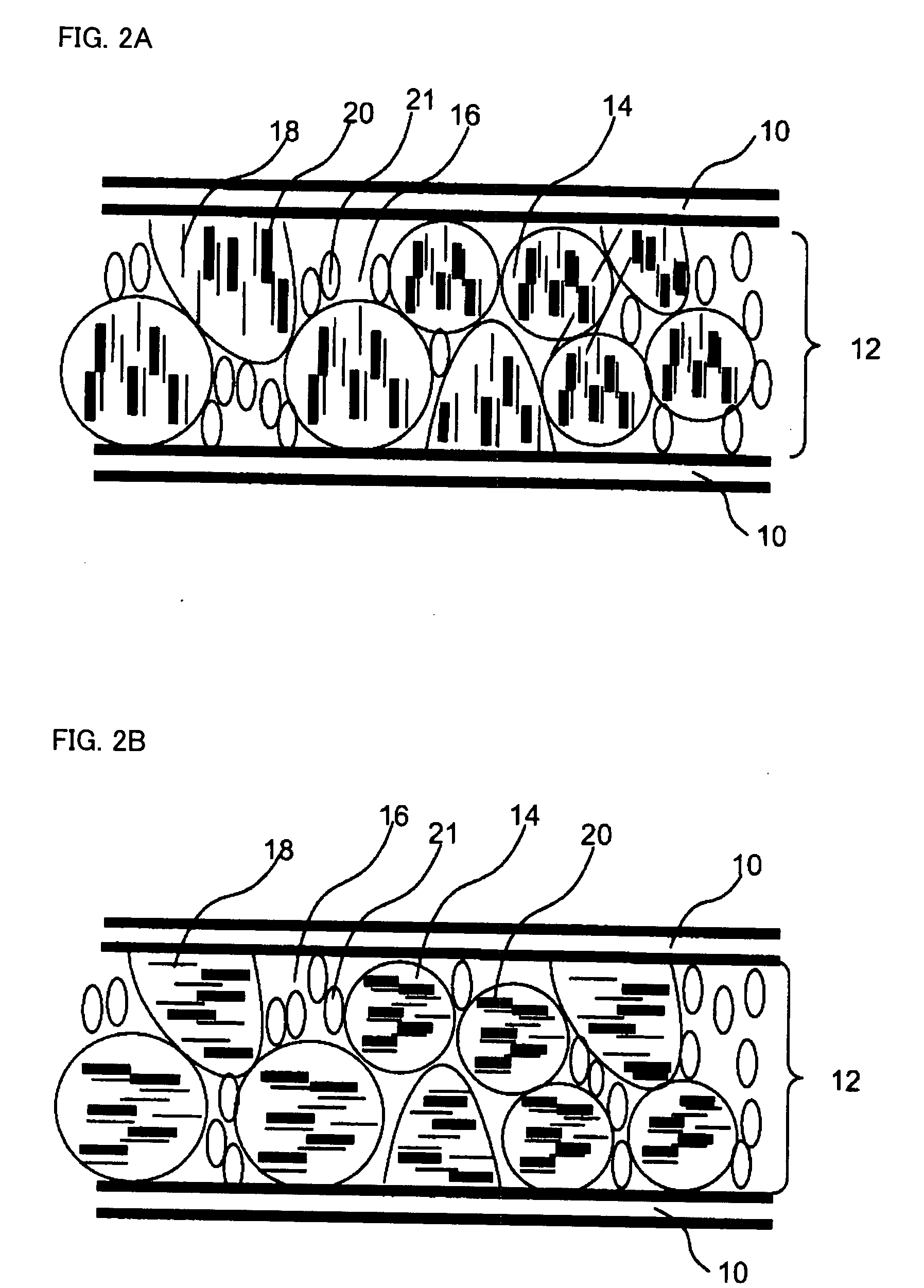
Light modulating material
- Summary
- Abstract
- Description
- Claims
- Application Information
AI Technical Summary
Benefits of technology
Problems solved by technology
Method used
Image

Examples
example 1
Preparation of Light Modulating Material
1. Preparation of Dichroic Dye and Liquid Crystal
[0166]Dichroic dyes (1-2) and (1-8) were synthesized according to the method disclosed in JP-A No. 2003-192664. A dichroic dye (1-13) was synthesized according to the method disclosed in JP-A No. 2005-120334. A yellow compound Y-1, a magenta compound M-1, and a cyan compound C-1 were synthesized according to the method disclosed in Jpn. J. Appl. Phys., Vol. 37, p. 3422 (1998).
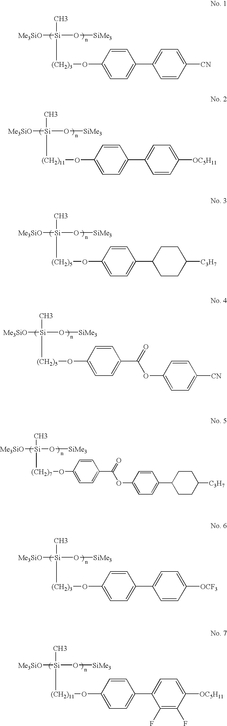
[0167]A host liquid crystal ZLI-2806 (a nematic liquid crystal) was purchased from Merck & Co. In addition, polymer materials No. 4 and No. 9 of the exemplary compounds were synthesized according to the following schemes.
2. Preparation of Light Modulating Material Using a Liquid Crystal composition Containing Dichroic Dye
[0168]A film having vertically aligned polyimide (manufactured by Nissan Chemical) was provided on a glass substrate having ITO, that is, on a transparent substrate, by spin coating and firing.
[0169]In 1.0 ...
example 2
Preparation of Light Modulating Material
1. Preparation of Plastic Substrate
[0174]An undercoat layer and a back layer were formed on PEN (trade name: Q65A, manufactured by Dupont-Teijin) in the same manner as in preparation of sample 110 in example 1 in JP-A No. 2000-105445. That is, 100 parts by weight of polyethylene-2,6-naphthalate polymer, and 2 parts by weight of Tinuvin P.326 (trade name, manufactured by Ciba-Geigy) as ultraviolet absorbent were dried, and dissolved at 300° C., extruded from a T-type die, and vertically drawn by 3.3 times at 140° C., and successively drawn laterally by 3.3 times at 130° C., and thermally fixed for 6 seconds at 250° C., and a plastic substrate (PEN) of the invention of 90 μm in thickness was obtained.
2. Preparation of Transparent Electrode Layer
[0175]On one side of the plastic substrate obtained above, conductive indium tin oxide (ITO) was applied, and a uniform thin film of 200 nm in thickness was laminated. The surface resistance was about 20 ...
example 3
[0189]A light modulating material of the invention was fabricated in the same manner as in Example 1, except that the host liquid crystal was changed to ZLI-6610 (trade name, manufactured by Merck & Co.), and that the vertically aligned layer was changed to an octadecyl silane coupling agent (manufactured by Shin-Etsu Kagaku Kogyo). The light modulating material of the invention was evaluated in the same way as in Example 1, and a high light modulating ability was confirmed. The light modulating material of the invention was in a transparent state of high transmissivity when no voltage was applied, and it was confirmed that power consumption could be reduced.
PUM
| Property | Measurement | Unit |
|---|---|---|
| Fraction | aaaaa | aaaaa |
| Fraction | aaaaa | aaaaa |
| Fraction | aaaaa | aaaaa |
Abstract
Description
Claims
Application Information
 - R&D Engineer
- R&D Manager
- IP Professional
- Industry Leading Data Capabilities
- Powerful AI technology
- Patent DNA Extraction
Browse by: Latest US Patents, China's latest patents, Technical Efficacy Thesaurus, Application Domain, Technology Topic, Popular Technical Reports.
© 2024 PatSnap. All rights reserved.Legal|Privacy policy|Modern Slavery Act Transparency Statement|Sitemap|About US| Contact US: help@patsnap.com