Wiring Circuit Board Producing Method and Wiring Circuit Board

a technology of wiring circuit board and producing method, which is applied in the direction of printed circuit manufacturing, printed circuit aspects, conductive pattern formation, etc., can solve the problem of non-uniform pattern of electric conductors, and achieve the effect of cost saving

Inactive Publication Date: 2007-09-27
CLUSTER TECH
View PDF7 Cites 25 Cited by
  • Summary
  • Abstract
  • Description
  • Claims
  • Application Information

AI Technical Summary

Benefits of technology

[0018] The wiring circuit board and the wiring circuit board producing method according to the present invention allow the electric conductor forming liquid to be inhibited from overflowing and turned to a high-density circuit of wiring. Particularly, the electric conductor forming liquid such as silver ink which is costly can be minimized in the consumption, thus contributing to the overall cost saving.
[0019] Other objects, features, and advantages of the present invention will be apparent from the following description in conjunction with the drawings.

Problems solved by technology

However, when the electrically conductive ink is applied into the grooves which is very narrow in the width, it may overflow and spill from the grooves, resulting in non-uniformity in the pattern of electric conductor.

Method used


Image

  • Wiring Circuit Board Producing Method and Wiring Circuit Board
  • Wiring Circuit Board Producing Method and Wiring Circuit Board
  • Wiring Circuit Board Producing Method and Wiring Circuit Board

Examples


first embodiment

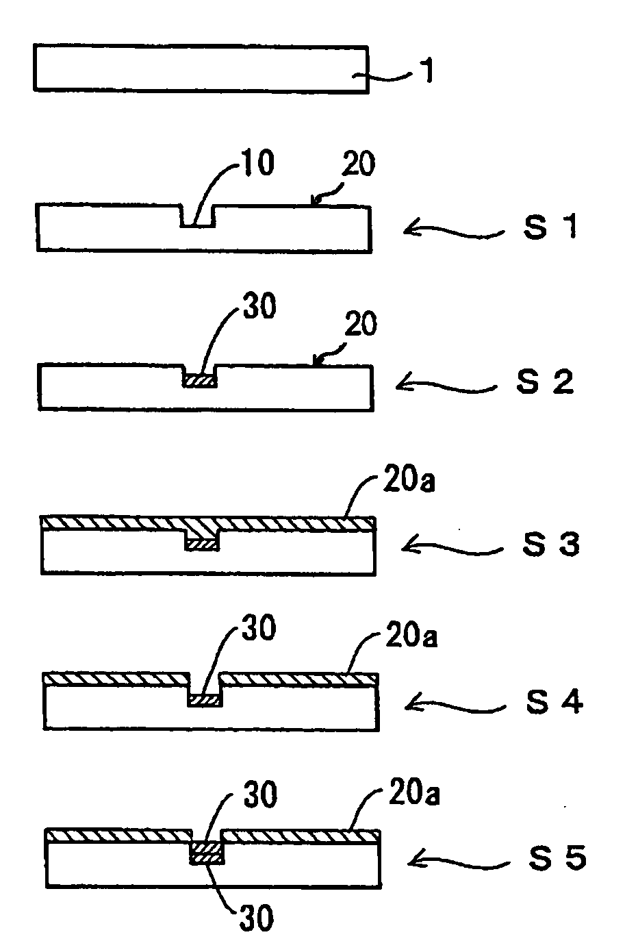
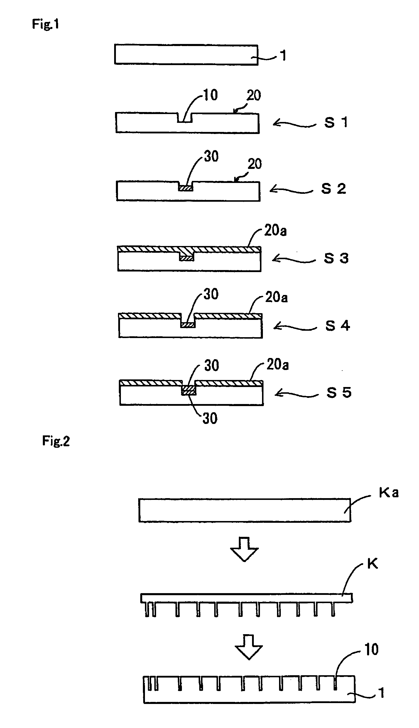
[0052] The present invention will be described in more detail, referring to the accompanying drawings. FIG. 1 is a cross sectional view illustrating steps of a wiring circuit board producing method as the present invention. The wiring circuit board producing method of this embodiment comprises a groove patterning step S1, an electric conductor forming liquid supplying step S2, a repellent layer providing step S3, a groove cleaning step S4, and another electric conductor forming liquid supplying step S5. Those steps are followed by a post-process step where the electric conductor forming liquid or conductive ink is heated and dried for solidification.

[0053] The material of a wiring substrate 1 in the embodiment is preferably, but not limited to, a not electrically conductive material which has OH groups exposed at the surface, as will be described later, and is subject to groove providing process for providing a pattern of grooves 10 with the use of offset-stamping or laser cutting. ...

seventh embodiment

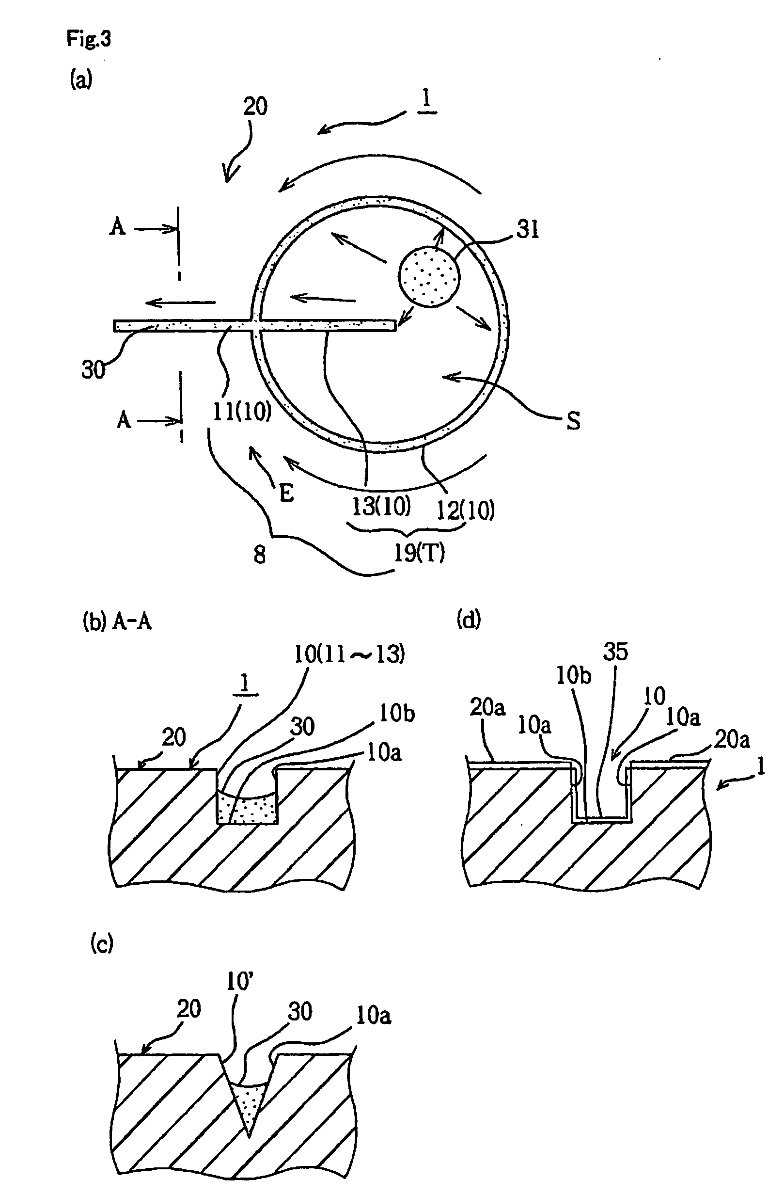
[0086] the present invention will be described where the electrically conductive ink 30 is replaced by a surface modifying solution, such as potassium hydroxide (KOH), as the electric conductor forming liquid. The grooves are filled up with the surface modifying solution by the action of capillarity. Then, a post-process follows for separating an electrically conductive material from the surface modifying solution in the grooves 10 by another electroless plating action or an electro-plating action after the electroless plating to deposit the patterned circuit along the opening of the grooves.

[0087] The post-process similar to that of the sixth embodiment is preceded by the electric conductor forming liquid supplying step S5 of the third or fourth embodiment and comprises a modifying solution removing step S10, an ion exchange reacting step S11, a copper thin layer depositing step S12, and a plating depositing step S13. This may also be implemented as the post-process following the s...

sixth embodiment

[0090] This is followed by the copper thin film depositing step S12 where the substrate on which the copper ions are accumulated is immersed into a sodium borohydride water solution or a di-methyl amine borane (DMAB) water solution to deposit a thin layer of copper at the opening of the grooves. Alternatively, the substrate may be immersed into an anatase type TiO2 colloid solution to aggregate a photo-catalyst in the grooves and then exposed to ultraviolet light for triggering a reducing reaction by which a thin layer of copper is deposited in the grooves. The thin layer is then thickened to a patterned circuit through an electroless copper plating action or a copper electro-plating action, similar to the action in the

[0091] The electric conductor forming liquid in the seventh embodiment is not limited to the potassium hydroxide solution but may be any other solution, e.g., where potassium hydroxide is dissolved in ethylene glycol or tetra-decane.

[0092] Further embodiments will be...


PUM

PropertyMeasurementUnit
widthaaaaaaaaaa
widthaaaaaaaaaa
widthaaaaaaaaaa

Abstract

A wiring circuit board and a method of producing the same are provided in which a desired pattern of wiring is provided at higher density while permitting no overflow from the grooves of an electroless plating catalyst containing solution and an electric conductor forming liquid such as silver ink.
The pattern of electric conductor is deposited by applying the electric conductor forming liquid into the grooves provided in a substrate and distributing the same along the grooves with the action of capillarity. The method starts with patterning the grooves in the surface of the substrate (S1), applying the electric conductor forming liquid into the grooves (S2), and coating the surface of the substrate with a layer of repellent liquid which is lower in the affinity with the electric conductor forming liquid (S3). This is followed by cleaning at least the grooves (S4) and then filling the grooves with the electric conductor forming liquid once again (S5). The electric conductor forming liquid applied into the grooves is then distributed throughout the grooves by the action of capillarity. When silver ink is used, the pattern of electric conductor is produced by repeating an action of applying and drying a number of times. Alternatively, the patter of electric conductor can be produced by an electroless plating technique or a combination of an electroless plating technique and an electro-plating technique for separating an electrical conductive material form the electric conductor forming liquid.

Description

TECHNICAL FIELD [0001] The present invention relates to a wiring circuit board and a method of producing the same. More particularly, the present invention relates to a wiring circuit board producing method for applying an electric conductor forming liquid into grooves provided in a substrate, filling the grooves with the electric conductor forming liquid by the action of capillarity, and converting the electric conductor forming liquid into a pattern of conductor at the succeeding step and a wiring circuit board produced by the foregoing method. BACKGROUND ART [0002] Such a wiring circuit board producing method is known as disclosed in Patent Citation 1. In the citation, a pattern of fine grooves are provided in a substrate with the use of dies and filled with electrically conductive ink which is an electrically conductive material to develop the pattern of wiring. A similar method is known as disclosed in Patent Citation 2. Patent Citation 1: Japanese Patent Laid-open Publication...

Claims


Application Information

Patent Timeline
Patent Type & Authority Applications(United States)
IPC IPC(8): H05K3/10H01K3/10
CPCH05K3/4614Y10T29/49155H05K2201/0367H05K2201/0373H05K2201/09036H05K2201/09045H05K2201/09472H05K2203/0709H05K2203/1173H05K2203/1189H05K2203/1476H05K1/0284H05K3/107H05K3/1258H05K3/182H05K3/246H05K3/3436H05K3/4007Y10T29/49165H05K2201/0347
Inventor KITAOKA, KENJIFUJIMOTO, TAKAYOSHI
Owner CLUSTER TECH
Why Eureka
Try Eureka