

Transparent Conductive Laminated Body and Transparent Touch-Sensitive Panel
a technology of touch-sensitive panel, which is applied in the direction of conductive layers on insulating supports, instruments, natural mineral layered products, etc., can solve the problems of insufficient flexural resistance, inability to enjoy flexibility of polymer films, and the structure of metallic compound layers might be broken upon receiving external stress, etc., to achieve the effect of improving the flexibility of the transparent conductive laminated body
- Summary
- Abstract
- Description
- Claims
- Application Information
AI Technical Summary
Benefits of technology
Problems solved by technology
Method used
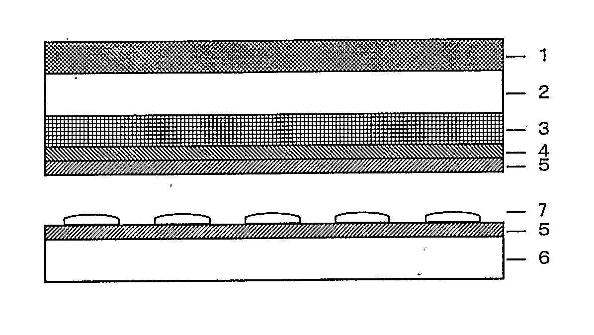
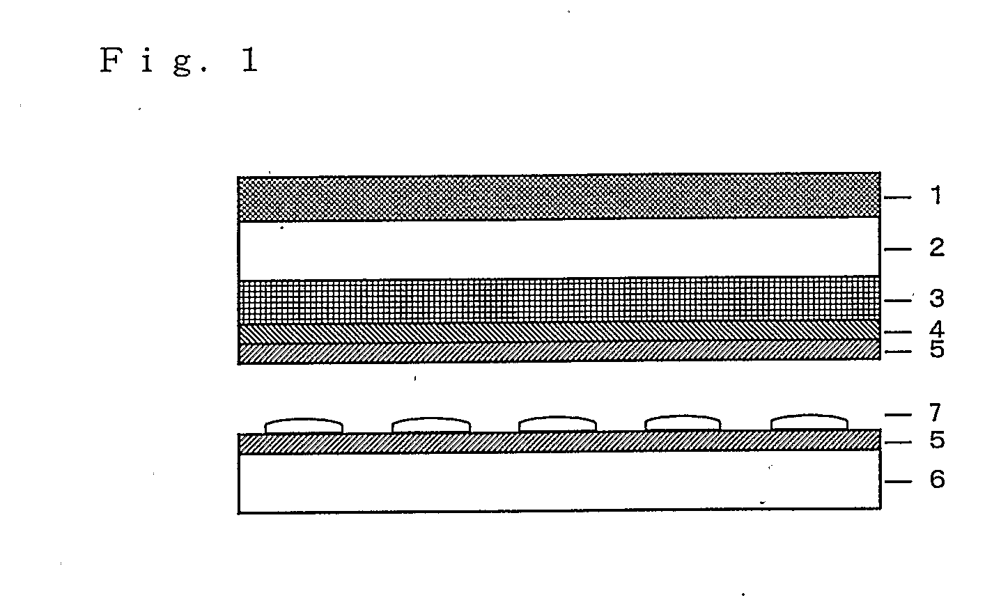
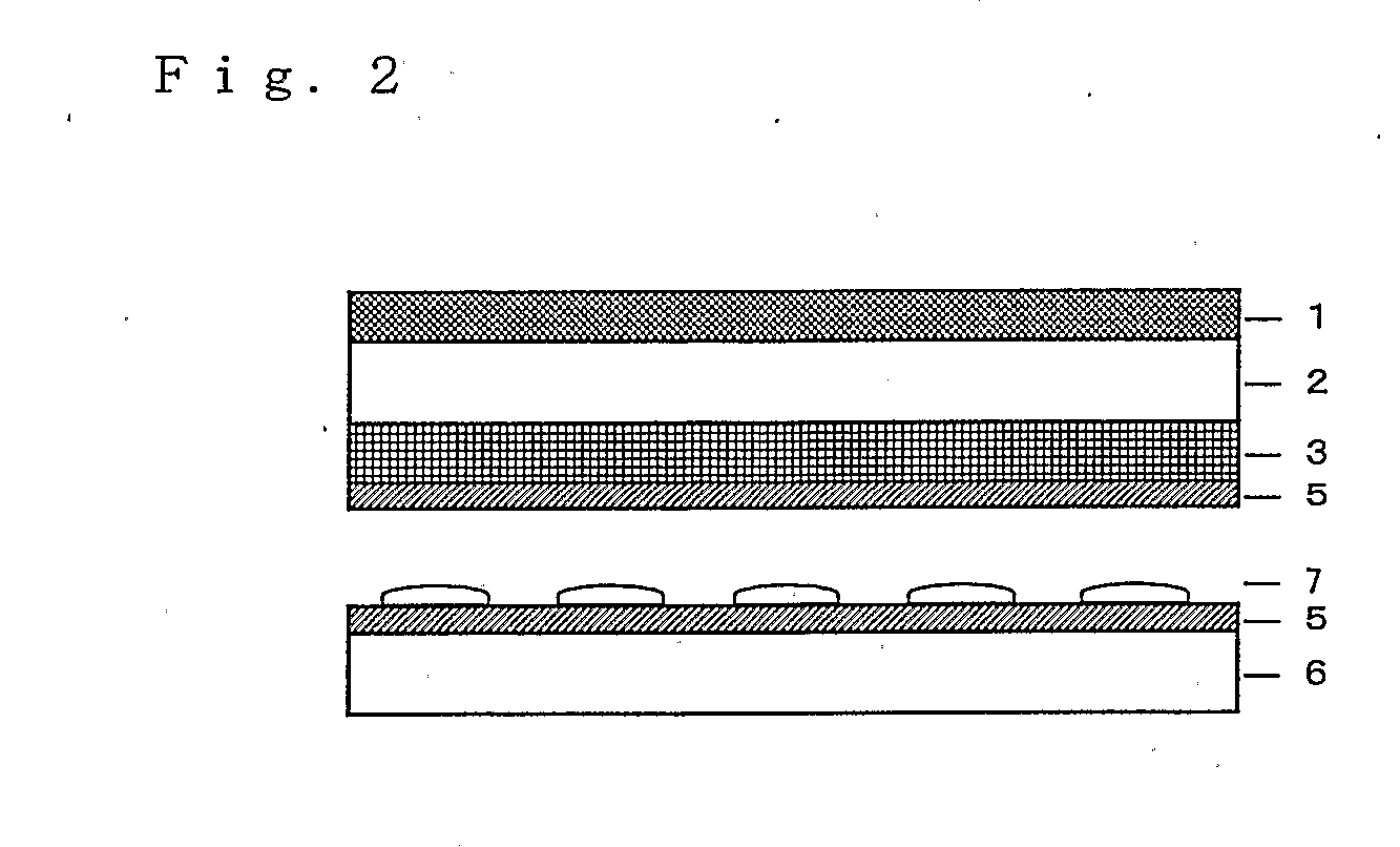
Image

Examples
example 1
[0127] As the polymer film, Pure-Ace WR, produced by Teijin Chemicals Ltd. was used. This is referred to as a polymer film A. As the cured resin component, an acrylate monomer having a fluorene skeleton (resin B), produced by Osaka Gas Chemicals Co., Ltd. and a polyfunctional urethane acrylate monomer (resin C), produced by Shin-Nakamura Chemical Co., Ltd., were used as a mixture. As an initiator, Irgacure 184 (initiator D), produced by Ciba Specialty Chemicals, Inc., was used.
[0128] The resin B and the resin C were mixed to a solid content weight ratio of 70 / 30 to obtain a cured resin component E. The cured resin component E was diluted with a mixed solvent of 1-methoxy-2-propanol (1M2P) and isopropyl alcohol (IPA) to a solid concentration of 20% by weight. The initiator D was added thereto to a solid content weight ratio of the cured resin component E and the initiator D of 100 / 5 to produce a coating composition. On one surface of the polymer film A having a refractive index at 5...
example 2
[0134] A cured resin layer having a thickness of 3 μm (having a refractive index at 550 nm of 1.62) was formed on the polymer film A having a refractive index at 550 nm or 1.65 in the same manner as in Example 1. An SiOx layer having a thickness of 5 nm was formed on the cured resin layer in the same manner as in Example 1. The refractive index at 550 nm of the SiOx layer was 1.50. The value x was about 1.6.
[0135] A transparent conductive layer having a thickness of 130 nm was formed on the SiOx layer in the same manner as in Example 1 to produce a transparent conductive laminated body.
[0136] The transparent conductive laminated body had a surface resistance of 28Ω / sq. and a transmittance of 86%. The adhesiveness of the transparent conductive layer was as good as 100 / 100. As a result of the flexural resistance test, the change in resistance was 1.05, and no crack was observed after the test, which indicated good flexural resistance.
[0137] The transparent conductive laminated body...
example 3
[0138] The resin B and the resin C were mixed at a solid content weight ratio of 70 / 30 to obtain a cured resin component E in the same manner as in Example 1. A dispersion liquid of silicon oxide fine particles F having an average primary particle diameter of 20 nm (produced by Fuso Chemical Co., Ltd., silicon oxide fine particle concentration: 10% by weight, dispersant: methyl ethyl ketone (MEK)) was prepared as the ultrafine particles C. A cured resin component G containing organosilane acrylate (UVICA AF#2, produced by Asai Bussan Co., Ltd.) was prepared as the organic compound containing silicon atoms. The cured resin component E, the dispersion liquid of silicon oxide fine particles F and the organic compound containing silicon atoms (cured resin component G) were mixed at a solid content weight ratio of 100 / 3 / 3, and diluted with a mixed solvent of 1-methoxy-2-propanol (1M2P) and isopropyl alcohol (IPA) to a solid concentration of 20% by weight. The initiator D was added theret...
PUM
| Property | Measurement | Unit |
|---|---|---|
| thickness | aaaaa | aaaaa |
| thickness | aaaaa | aaaaa |
| average primary particle diameter | aaaaa | aaaaa |
Abstract
Description
Claims
Application Information