
Method and system for controlling semiconductor manufacturing apparatus

a manufacturing apparatus and semiconductor technology, applied in the field of method and system control of semiconductor manufacturing apparatus, can solve the problems of rare to keep the manufacturing apparatuses in non-stop operation, large energy loss, and inability to supply electric power to the units, and achieve the effects of reducing energy loss, reducing energy loss in the wait mode of the apparatus, and increasing energy consumption

Inactive Publication Date: 2007-10-04
SEIKO EPSON CORP
View PDF1 Cites 27 Cited by
  • Summary
  • Abstract
  • Description
  • Claims
  • Application Information

AI Technical Summary

Benefits of technology

[0011]An advantage of the invention is to provide a method and system for controlling semiconductor manufacturing apparatuses, and particularly to a technique to reduce energy loss when the semiconductor manufacturing apparatuses are in a wait mode, without interfering with turnaround-time (TAT) reduction.
[0012]According to a first aspect of the invention, a method for controlling a semiconductor manufacturing apparatus in a wait mode includes: obtaining information regarding a waiting time required for a product to arrive at the apparatus on a production line, the product being subjected to a predetermined process by the semiconductor manufacturing apparatus; obtaining information regarding a time required to control energy saving between lowering electric power and other energy used by the semiconductor manufacturing apparatus in the wait mode to a level at which the processing is not ready and raising the electric power and the other energy to a processable level at which the product processing is ready; and judging whether or not to execute the energy saving control of the semiconductor manufacturing apparatus based on results of comparison of the required time with the waiting time and of estimation on an effect of energy saving obtained by executing the energy saving control during the waiting time.
[0013]Examples of the “semiconductor manufacturing apparatus” include a dry etching apparatus, a CVD apparatus, and a thermal treatment apparatus. The apparatus receives the electric power and the other energy as consumption energy. Examples of the “product” include a semiconductor device formed on a wafer or a glass substrate. The “electric power and other energy in a wait mode” refers to the electric power and the other energy used by the semiconductor manufacturing apparatuses in the wait mode between production processes, for example. The “other energy” refers to energy other than the electric power, such as evacuated air, cooling water, compressed air, vacuum, nitrogen (N2), and released heat. The “processable level” is a level at which processing is ready as soon as the product to be processed is provided to a loader of the manufacturing apparatus.
[0014]In the first aspect of the invention, the energy saving control may be executed only if the waiting time in the wait mode of the semiconductor manufacturing apparatus is longer than the time required for the energy saving control and if the energy consumption in the wait mode is estimated to decrease due to the execution of the energy saving control during the waiting time. Therefore, the energy loss in the wait mode of the apparatus may be reduced without interfering with the TAT reduction.
[0015]It is preferable that the judgment on whether or not to execute the energy saving include: executing the energy saving control if the required time is shorter than the waiting time and if it is estimated that an amount of energy consumption in a wait mode will decrease due to the execution of the energy control during the waiting time; and not executing the energy saving control if the required time is equal to or longer than the waiting time or if it is estimated that an amount of energy consumption in a wait mode will not decrease due to the execution of the energy control during the waiting time.
[0016]In the energy saving control of e.g., the thermal treatment apparatus, the temperature of the furnace (reaction chamber) may be lowered and then returned to the original temperature after a predetermined period of time by heating inside the furnace. However, it requires energy to raise the once lowered temperature in the furnace to the original temperature. Therefore, if the step of maintaining the temperature inside the furnace of the energy saving control at a low temperature finishes in a short period of time, it is probable that the energy consumption even increases because of the energy saving control.

Problems solved by technology

The apparatus does not supply electric power to the units in the waiting mode.
Therefore, it is rare to keep the manufacturing apparatuses in non-stop operation between predetermined maintenance breaks.
Therefore, if the waiting time is long, there is a large loss of energy.
However, it requires energy to raise the once lowered temperature in the furnace to the original temperature.
Therefore, if the step of maintaining the temperature inside the furnace of the energy saving control at a low temperature finishes in a short period of time, it is probable that the energy consumption even increases because of the energy saving control.
In this case, because the semiconductor manufacturing apparatus is normally designed so that the processable level is maintained, it is possible that, once the electric power and the other power in the wait mode fall to the low energy level, the apparatus may not rise easily to the processable level thereafter.
In other words, a change in the states of the semiconductor manufacturing apparatus may accompany a risk of having to recover the state of the apparatus.

Method used


Image

  • Method and system for controlling semiconductor manufacturing apparatus
  • Method and system for controlling semiconductor manufacturing apparatus
  • Method and system for controlling semiconductor manufacturing apparatus

Examples


Embodiment Construction

[0049]Embodiments of the invention will now be described with reference to the drawings.

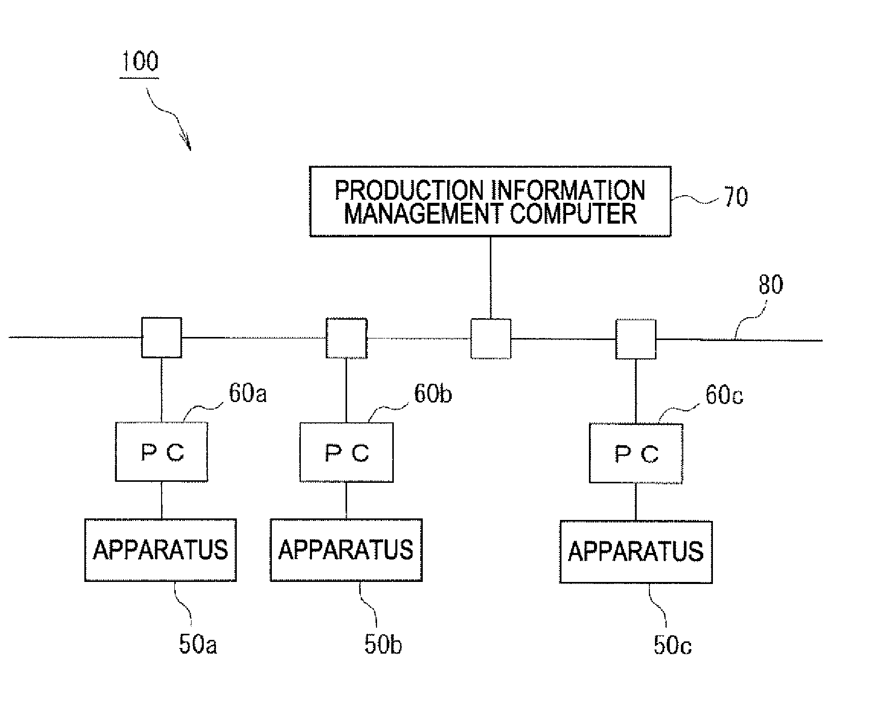
[0050]FIG. 1 schematically shows an example structure of a control system 100 of a semiconductor manufacturing apparatus according to the embodiments of the invention.

[0051]Referring to FIG. 1, the control system 100 includes: a plurality of semiconductor manufacturing apparatuses (hereunder referred to simply as manufacturing apparatuses) 50a, 50b, 50c, etc. arranged on a semiconductor devices production line, personal computers (hereunder referred to as PC) 60a, 60b, 60c, etc. each arranged corresponding to each of the manufacturing apparatuses 50, for example, a production information management computer 70 that manages production information of the products on the production line, and signal lines 80 that connect the PCs 60a, 60b, 60c, etc. to each other and send / receive data between the production information management computer 70 and the PCs 60a, 60b, 60c, etc.

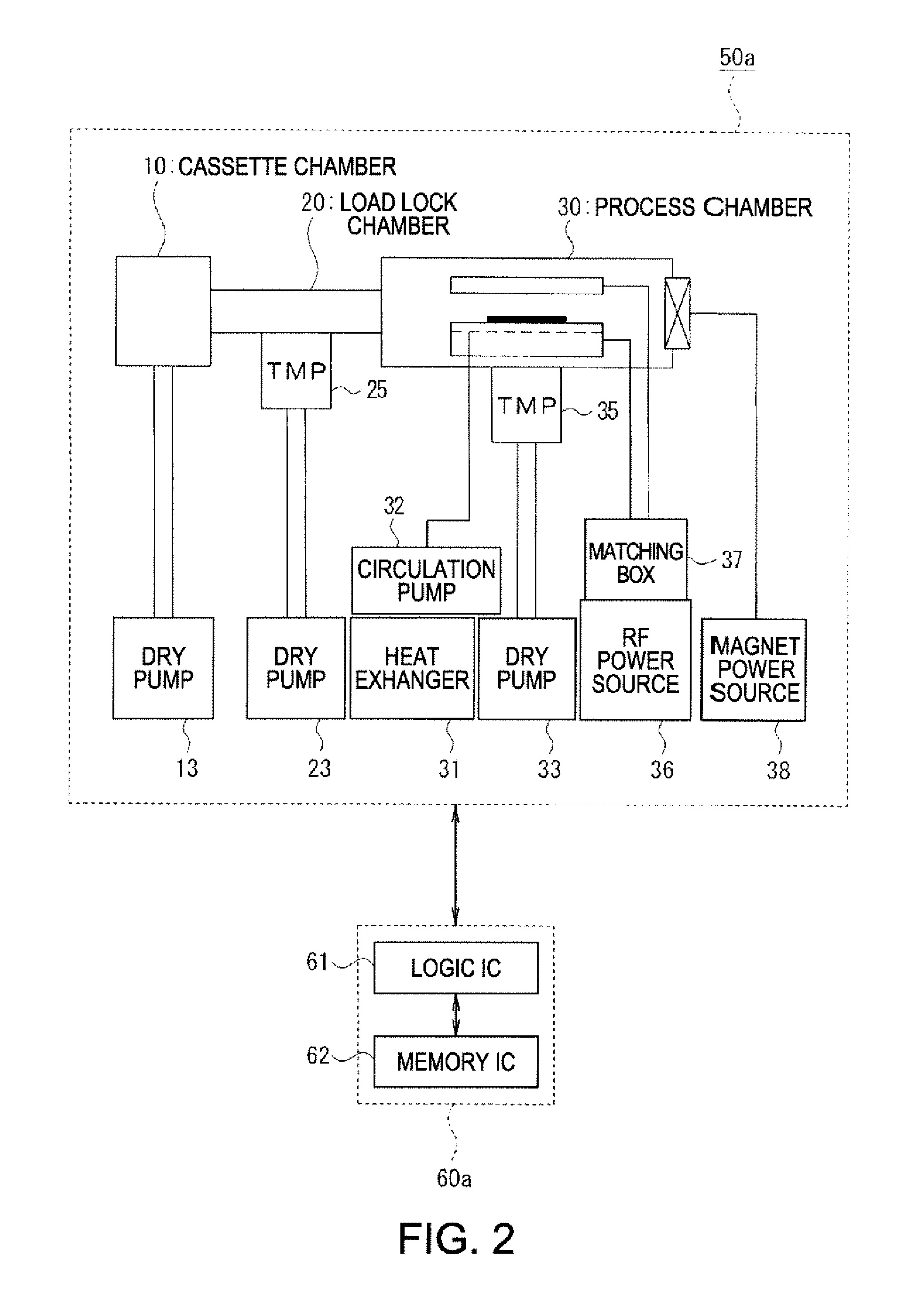
[0052]Examples of the manufac...


PUM


Abstract

A method for controlling a semiconductor manufacturing apparatus in a wait mode, including: obtaining information regarding a waiting time required for a product to arrive at the apparatus on a production line, the product being subjected to a predetermined process by the semiconductor manufacturing apparatus; obtaining information regarding a time required to control energy saving between lowering electric power and other energy used by the semiconductor manufacturing apparatus in the wait mode to a level at which the processing is not ready and raising the electric power and the other energy to a processable level at which the product processing is ready; and judging whether or not to execute the energy saving control of the semiconductor manufacturing apparatus based on results of comparison of the required time with the waiting time and of estimation on an effect of energy saving obtained by executing the energy saving control during the waiting time.

Description

BACKGROUND[0001]1. Technical Field[0002]The present invention relates to a method and system for controlling semiconductor manufacturing apparatuses, and particularly to a technique to reduce energy loss when the semiconductor manufacturing apparatuses are in a wait mode, without interfering with turnaround-time (TAT) reduction.[0003]2. Related Art[0004]A production line of semiconductor devices has a clean room that makes filtered clean air flow down and various manufacturing apparatuses arranged in the clean room. Examples of the apparatuses are: a thermal treatment apparatus that generates thermal diffusion of an impurity in a semiconductor wafer, a chemical-vapor deposition (CVD) apparatus that provides an insulating film, and a dry etching apparatus that etches an insulating film or a conductive film. Most of the apparatuses require not only electric power but also other energy such as evacuated air, cooling water, compresses air, vacuum, nitrogen (N2), and released heat.[0005]...

Claims


Application Information

Patent Timeline
IPC IPC(8): B05C11/00
CPCG05B19/41865H01L21/67276G05B2219/45031G05B2219/32021Y02P70/10Y02P70/50Y02P80/10Y02P90/02
Inventor TOMINE, TETSU
Owner SEIKO EPSON CORP
Features
  • Generate Ideas
  • Intellectual Property
  • Life Sciences
  • Materials
  • Tech Scout
  • Unparalleled Data Quality
  • Higher Quality Content
  • 60% Fewer Hallucinations
Learn More