High-sensitivity surface detection system and method
Inactive Publication Date: 2007-10-04
ARIST INSTR
View PDF51 Cites 39 Cited by
Summary
Abstract
Description
Claims
Application Information
AI Technical Summary
This helps you quickly interpret patents by identifying the three key elements:
Problems solved by technology
Method used
Benefits of technology
[0017] The present invention solves the aforementioned problems by providing a system and method for improved parti
Problems solved by technology
Particles constitute unwanted contamination.
The detection of such small defects on a 300 mm wafer by optical means at such high throughputs and accuracies is a major challenge.
Smaller illuminating NA's result in larger illuminating areas, and thus lower power densities.
As stated above, smaller illuminating lens NA's result in larger illuminating areas, and lower power densities.
However they have considerable difficulties in detecting
Method used
Image
Click on the blue label to locate the original text in one second.
Reading with bidirectional positioning of images and text.
Examples
Embodiment Construction
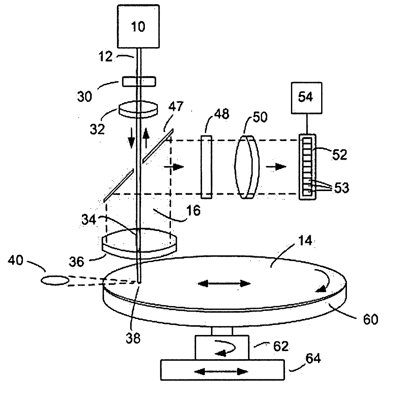
[0041] Described herein is a high-sensitivity wafer inspection system and method that provides improved surface detection accuracy and throughput. An optical configuration of the system is illustrated in FIG. 4. A collimated light source 10 (e.g. a laser source) produces a probe beam 12, which is shaped by lens assembly 32. Probe beam 12 passes through (or around) a spatial filter 46 (preferably positioned at the Fourier plane of lens 36). Probe beam 12 is shaped by lens assembly 32, into a narrow ellipse 34 at the entrance pupil of lens 36. The narrow ellipse 34 may be offset from the center axis of lens 36 to increase the angles of incidence for the probe beam onto the wafer. Lens 36 then focuses the probe beam 12 onto a sample surface 14 in the form of an illuminated stripe 38. For clarity, the illuminated stripe 38 is illustrated in larger size as 40. The long axis of stripe 38 is radial to the wafer as shown by 40. The specularly reflected illumination beam 42 from the sample s...
PUM
Abstract
An inspection system and method for inspecting a sample surface, with a light source for generating a probe beam of light, a high NA lens for focusing the probe beam onto a sample surface, and collecting a scattered probe beam from the sample surface, optics for imaging the scattered probe beam onto a detector having a plurality of detector elements that generate output signals in response to the scattered probe beam, and a processor for analyzing the output signals to identify defects on the sample surface. Shaping the beam into a stripe shape increases intensity without sacrificing throughput. Offsetting the beam from the center of the high NA lens provides higher angle illumination. Crossed polarizers also improve signal quality. A homodyne or heterodyne reference beam (possibly using a frequency altering optical element) can be used to create an interferometric signal at the detector for improved signal to noise ratios.
Description
[0001] This application claims the benefit of the following U.S. Provisional Applications: 60 / 776,037, filed Feb. 22, 2006; 60 / 777,796, filed Feb. 28, 2006; 60 / 795,836, filed Apr. 27, 2006; 60 / 810,561, Filed Jun. 1, 2006; 60 / 836,786, filed Aug. 9, 2006; 60 / 850,038, filed Oct. 6, 2006; and 60 / 859,846, filed Nov. 16, 2006; all of which are incorporated herein by reference in their entirety.FIELD OF THE INVENTION [0002] The present invention relates to nondestructive inspection of surfaces, and in particular to the optical inspection of semiconductor wafers for defects. BACKGROUND OF THE INVENTION [0003] Optical inspection of semiconductor wafers is a critical requirement for process development, manufacturing ramp-up, yield improvement and ongoing quality control. While the focus of this disclosure concerns semiconductor wafer inspection, the innovations herein can also be applied to other areas as well, such as flat-panel and memory media inspection. [0004] In semiconductor manufactu...
Claims
Application Information
Patent Timeline
Application Date:The date an application was filed.
Publication Date:The date a patent or application was officially published.
First Publication Date:The earliest publication date of a patent with the same application number.
Issue Date:Publication date of the patent grant document.
PCT Entry Date:The Entry date of PCT National Phase.
Estimated Expiry Date:The statutory expiry date of a patent right according to the Patent Law, and it is the longest term of protection that the patent right can achieve without the termination of the patent right due to other reasons(Term extension factor has been taken into account ).
Invalid Date:Actual expiry date is based on effective date or publication date of legal transaction data of invalid patent.