Optical/electrical circuit interconnect board and evaluation method therefor

a technology of optical/electrical circuits and interconnect boards, applied in the direction of optical elements, optical waveguide light guides, instruments, etc., can solve the problems of increasing packaging areas or manufacturing costs, noise or signal delay, and more and more, so as to improve alignment accuracy, reduce cost, and facilitate mounting

Inactive Publication Date: 2007-10-04
THE FUJIKURA CABLE WORKS LTD +1
View PDF5 Cites 50 Cited by
  • Summary
  • Abstract
  • Description
  • Claims
  • Application Information

AI Technical Summary

Benefits of technology

[0013] The present invention has been achieved in view of the above-mentioned circumstances, and has a first object to provide an optical/electrical interconnect board comprising optical fibers that can be easily mounted with in...

Problems solved by technology

However, making the transmission rate in information by use of an electrical circuit faster results in problems such as noise or signal delay.
Therefore, it is becoming more and more difficult to actualize an electrical circuit with a transmission rate faster than ever, Furthermore, even if a faster transmission rate is indeed actualized by use of an electrical circuit, there is a concern that it will bring about problems of an increase in packaging areas or manufacturing costs caused by the necessity for a complex electric circuit or an extra shield against noise.
Furthermore, an optical/electrical interconnect is more often used for movable portions such as will be bent or twisted since consumer electric products come to have more functions and more complex designs.
However, the manufacturing processes thereof are very complicated and it is difficult to ...

Method used


Image

  • Optical/electrical circuit interconnect board and evaluation method therefor
  • Optical/electrical circuit interconnect board and evaluation method therefor
  • Optical/electrical circuit interconnect board and evaluation method therefor

Examples


example 1

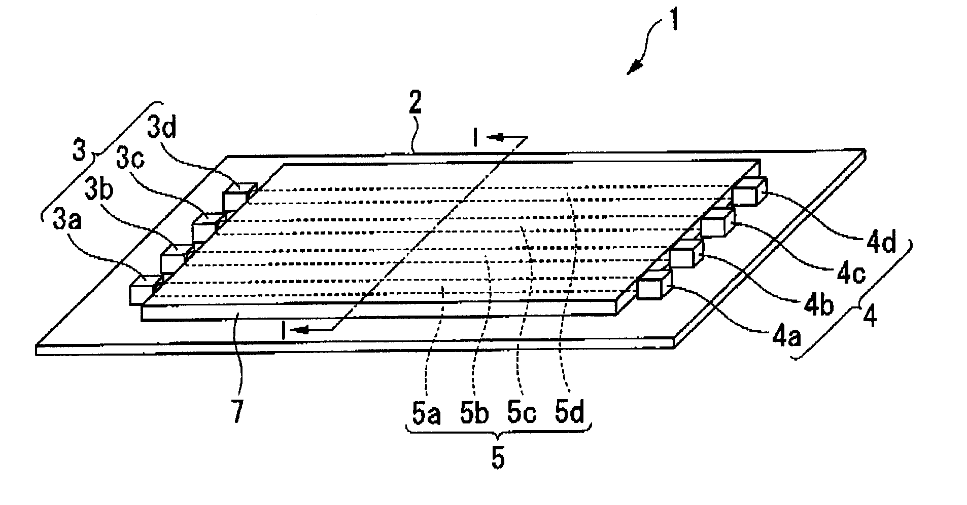
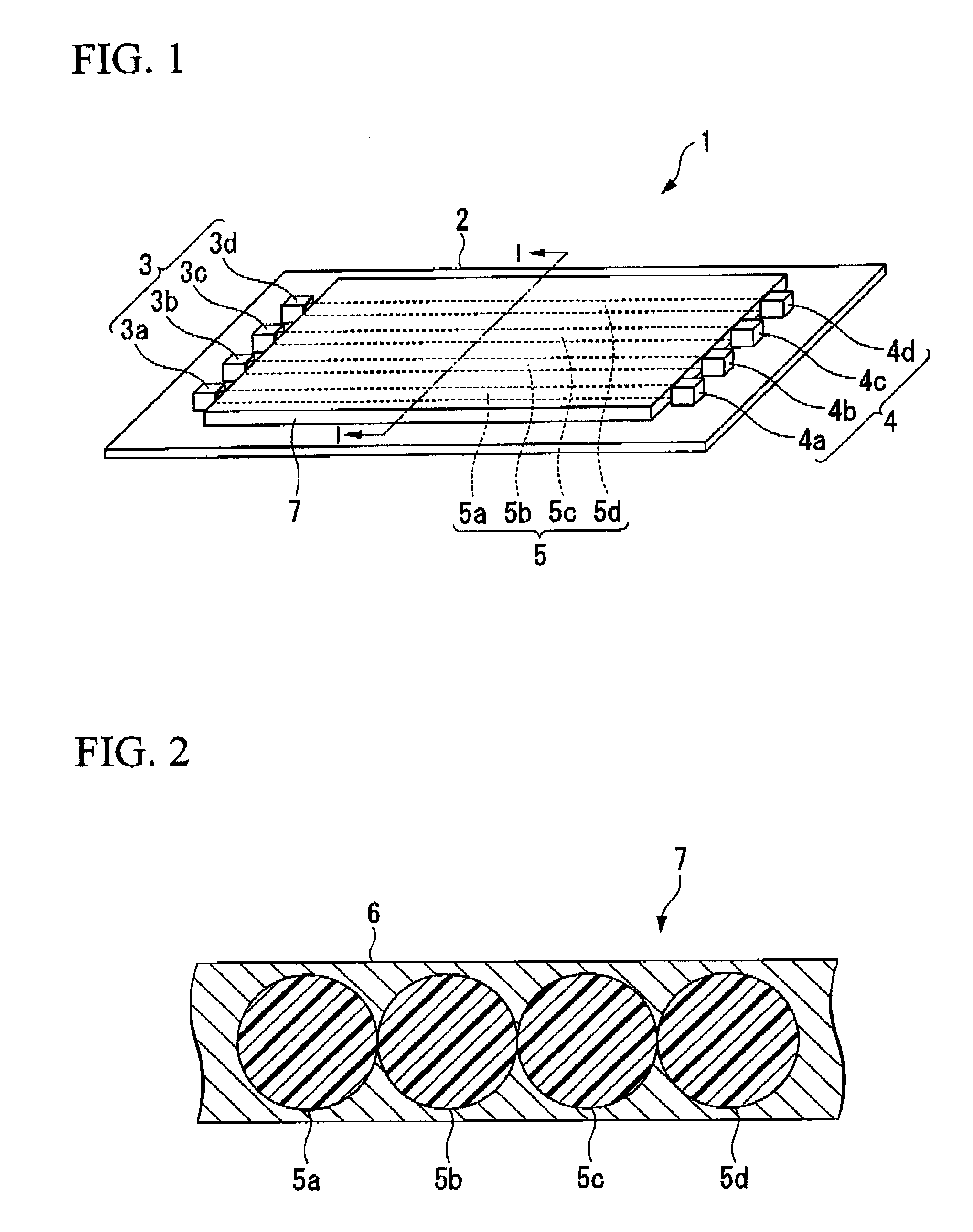
[0116] Next, to confirm that plastic optical fibers in the plastic optical tape are required to be arranged in straight lines, a planarity of the case as shown in FIG. 7B was evaluated where, in an optical fiber tape 7 with four plastic optical fibers 5a, 5b, 5c, 5d arranged in parallel with one another, one fiber 5b of the inner two plastic optical fibers 5b, 5c is upwardly displaced and the other fiber 5c is downwardly displaced. The planarity was obtained as a maximum value among distances from a line (hereinafter, referred to as reference line) 10 connecting the outer circumferences of the two plastic optical fibers 5a, 5d, at both ends of the optical fiber tape 7 to the outer circumferences of the plastic optical fibers 5b, 5c. Note that the plastic optical fibers 5 have a length of 1000 mm.

[0117] Light receiving intensity at light receiving elements was evaluated at planarities of 10 μm, 30 μm, 50 μm, and 100 μm. The results are shown in Table 1.

TABLE 1Light Intensity [dBm]...

example 2

[0120] Next, to confirm that replacing one or more of the plastic optical fibers in the optical fiber tape with the reinforcing wire member(s) can improve a planarity with good repeatability, four optical fiber tapes 57A, 57B, 57C, 57D, as shown in FIGS. 12 to 15 were manufactured. In the optical fiber tapes 57A, 57B, 57C, 57D, six plastic optical fibers are arranged in parallel with one another, and reinforcing wire members are located such that the number of adjacent plastic optical fibers is four, three, two, and one, respectively.

[0121] That is, in FIG. 11, outermost plastic optical fibers are relocated by reinforcing wire members 9a, 9b, respectively such that four optical fibers are adjacent to each other. In FIG. 12, an outermost plastic optical fiber at one end and a second outermost plastic optical fiber at the other end are relocated by reinforcing wire members 9a, 9b such that three plastic optical fibers are adjacent to each other. In FIG. 13, an outermost plastic optic...

example 3

[0125] Next, to confirm that when applied to a movable portion, an optical fiber tape with a reinforcing wire member comes to have strong resistance to repetitive bending or twisting by accurately adjusting the wire diameter (outer diameter) of the reinforcing wire member, an optical fiber tape 67 as shown in FIG. 15 was manufactured as follows: two glass optical fibers 69a, 69b were formed by previously coating a second coat material 65 on the outer circumferences of glass optical fibers 69 with a diameter of 125 μm as reinforcing wire members to make the outer diameter thereof equal to the wire diameter of plastic optical fibers 5 with a diameter of 500 μm; the glass optical fibers 69a, 69b were adjacently arranged in parallel to each other; plastic optical fibers 5a, 5b were located on the outer sides of the glass optical fibers 69a, 69b, one for each side; and these four fibers were brought together side-by-side and were coated with a first coating material 6.

[0126] The optical...


PUM


Abstract

An optical/electrical interconnect board includes a base material composing an electrical circuit; a plurality of light receiving/emitting units, each of the units being constituted by a light emitting element and a light receiving element packaged on the base material; and an optical fiber tape that connects the light emitting element to the light receiving element for each of the light receiving/emitting units, the optical fiber tape being formed by bringing together optical wires for the units in a side-by-side manner and coating with a first coating material.

Description

BACKGROUND OF THE INVENTION [0001] 1. Field of the Invention [0002] The present invention relates to an optical / electrical interconnect board in which optical fibers are packaged, in combination with electrical circuits, on a substrate packaged with a plurality of light receiving / emitting units constituted by light emitting elements and light receiving elements, and to an evaluation method of the coupling efficiency of the optical fibs constituting the optical / electrical interconnect board. [0003] Priority is claimed on Japanese Patent Application Nos. 2006-93333, filed Mar. 30, 2006, and 2007-085881, filed Mar. 28, 2007, the contents of which are incorporated herein by reference. [0004] 2. Description of the Related Art [0005] Inside electronic equipments currently in wide use such as cellular phones, digital still cameras, and television sets, a vast multitude of electric circuits are used for transmission of a variety of information including signals of a control system and image...

Claims


Application Information

Patent Timeline
IPC IPC(8): G02B6/12G02B6/36G02B6/44H01L33/62
CPCG02B6/4249G02B6/4403G02B6/43G02B6/12
Inventor FUKUDA, TAKESHIICHII, KENTAROTERADA, YOSHIHIROFUJIMAKI, MUNEHISAOKA, HIROYUKIFURUKAWA, YOSHIKIINUZUKA, KATSUMI
Owner THE FUJIKURA CABLE WORKS LTD
Why Eureka
Try Eureka