LSI circuit designing system, antenna damage preventing method and prevention controlling program used in same

Inactive Publication Date: 2007-10-04
NEC CORP
View PDF1 Cites 11 Cited by
  • Summary
  • Abstract
  • Description
  • Claims
  • Application Information

AI Technical Summary

Benefits of technology

[0047]With the above configurations, the wiring segment expected to cause antenna damage to a gate insulating film (for example, the gate oxide film in each of MOS transistors) due to an antenna effect in which the wiring segment absorbs electric charges generated during plasma etching processes is detected by the gate sizing means and an area of the gate electrode of each of the MIS transistors connected to the detected wiring segment is corrected (that is, gate-sized) to become a value enabling the prevention of antenna damage occurring in the gate insulating film of each of the MIS transistors and, therefore, antenna damage can be prevented without shortening a length of the uppermost layer wiring providing advantages in terms of low resistance and design for delay. The above gate-sizing process makes it unnecessary to perform designing of diodes with only the aim of preventing the antenna damage

Problems solved by technology

Conventionally, in wiring metal layer processing at a time of manufacturing semiconductor integrated circuits such as LSIs, there are some cases in which a wiring segment, due to the reason that it erroneously operates as an antenna, absorbs electrostatic charges during the processing of plasma etching, which is then discharged, when the charges exceed a specified level, through a gate electrode of each of MOS transistors connected to the above wiring segment and, as a result, the electrostatic charges cause damage to a gate oxide film o

Method used


Image

  • LSI circuit designing system, antenna damage preventing method and prevention controlling program used in same
  • LSI circuit designing system, antenna damage preventing method and prevention controlling program used in same
  • LSI circuit designing system, antenna damage preventing method and prevention controlling program used in same

Examples


first embodiment

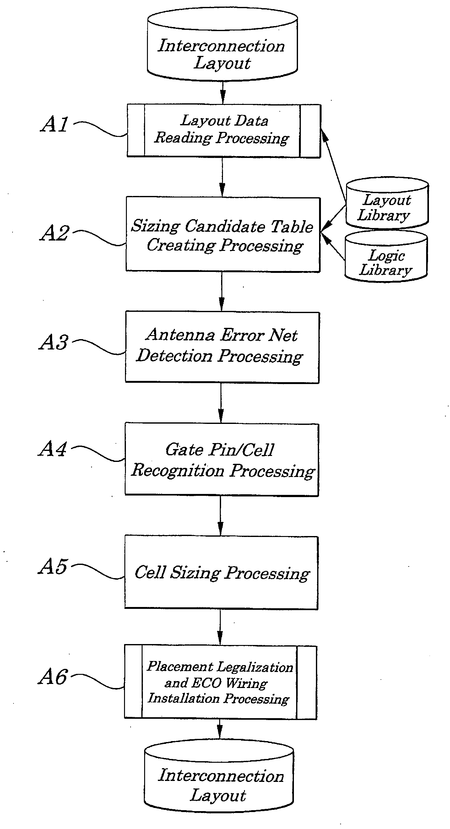
[0071]FIG. 3 is a block diagram showing configurations of main components making up an (Large-Scale Integrated) LSI circuit designing system of the first embodiment of the present invention. In FIG. 1, a processing number for the flow chart is assigned to each block as a reference number. The LSI circuit designing system of the first embodiment, as shown in FIG. 3, includes a data processing device 11 and a storage device 2, by inputting circuit information corresponding to circuit configurations in the LSI made up of MOS (Metal Oxide Semiconductor) transistors, layout design corresponding to the circuit configuration is carried out. The storage device 2 is made up of a hard disk to permanently store information or a like and includes a wiring layout storing unit 21, a layout library 22, a logic library 23, and a wiring layout storing unit 24. The wiring layout storing unit 21 stores layout information free from a DRC (Design Rule Checking) error obtained after the completion of des...

second embodiment

[0092]FIG. 10 is a block diagram showing configurations of main components making up the LSI circuit designing system according to the second embodiment of the present invention. In FIG. 10, same reference numbers are assigned to components having the same function as in the first embodiment and their descriptions are omitted accordingly. The LSI circuit designing system of the second embodiment, as shown in FIG. 10, includes, instead of the data processing device 1 and storage device 2 shown in FIG. 3, a data processing device 1A having configurations being different from those in the first embodiment and a storage device 2A. The data processing device 1A has a layout reading means 11, an antenna error net detecting means 13, an error net sequential processing means 14, an error preventing cell connecting means 19, an antenna error net detecting means 13A, an error net termination judging means 17, and a placement legalization / ECO wiring installing means 18. The sizing candidate ta...


PUM


Abstract

An LSI (Large-Scale Integrated) circuit system capable of preventing antenna damage occurring in MOS (Metal Oxide Semiconductor) transistors due to an erroneous operation of a wiring formed during manufacturing processes of LSIs or like as an antenna. Layout data after installation of wirings is read by layout reading processing and up-sizing candidate table is created by sizing candidate table creating processing using various libraries so that candidate values are arranged for every function cell in ascending order of gate areas. By antenna error net detecting processing, a net having wiring layers causing an antenna error is detected. A gate pin, its instance, type of a cell connected to the net is recognized by gate pin/cell recognizing processing and a cell enabling prevention of an antenna error is up-sized by cell sizing processing by referring to a gate area stored in an up-sizing candidate table.

Description

BACKGROUND OF THE INVENTION[0001]1. Field of the Invention[0002]The present invention relates to an LSI (Large-Scale Integrated) circuit designing system, an antenna damage preventing method, and an antenna damage prevention controlling program used in the LSI circuit designing system and more particularly to the LSI circuit designing system suitably used in the LSI circuit designing system capable of preventing antenna damage, which is caused by a wiring erroneously operating as an antenna in some cases formed during processes of manufacturing a semiconductor integrated circuit such as the LSI, occurring in a gate insulating film (for example, a gate oxide film of a MOS [Metal Oxide Semiconductor]) transistor making up a MIS (Metal Insulator Semiconductor) transistor mounted internally in the LSI, to the antenna damage preventing method and to the antenna damage prevention controlling program to be used for the LSI circuit designing system.[0003]The present application claims prior...

Claims


Application Information

Patent Timeline
IPC IPC(8): G06F17/50
CPCG06F17/5077G06F2217/12G06F17/5081G06F30/394G06F2119/18G06F30/398Y02P90/02
Inventor ONO, KOKI
Owner NEC CORP
Why Eureka
Try Eureka