Wafer processing apparatus capable of controlling wafer temperature

a technology of processing apparatus and wafer, which is applied in the direction of electrical apparatus, electrical discharge tubes, basic electric elements, etc., can solve the problems of inability to reduce the temperature variation between the wafers and the inability to reduce the temperature variation over the wafers that are sequentially processed, and achieves great temperature dependence and high reproducibility.

Inactive Publication Date: 2007-10-18
KANNO SEIICHIRO +8
View PDF2 Cites 2 Cited by
  • Summary
  • Abstract
  • Description
  • Claims
  • Application Information

AI Technical Summary

Benefits of technology

[0018] According to the invention, since the wafer temperature variation can be reduced within the lot, wafers can be processed with high reproducibility even when the invention is applied to the process having great temperature dependence.

Problems solved by technology

The prior art described in the above JP-A-6-124916 does not consider the point that the wafers are continuously processed in turn, and it has the drawback that the temperature variation between the wafers cannot be reduced.
That is, in the prior art, the temperature variation can be reduced during the time in which each wafer is being processed, but it cannot be reduced over the wafers that are sequentially processed.
Therefore, in the actual process line, the wafers even within the same lot, for example, the first wafer and the twenty-fifth wafer, most probably have different etching results, thus causing a trouble.

Method used


Image

  • Wafer processing apparatus capable of controlling wafer temperature
  • Wafer processing apparatus capable of controlling wafer temperature
  • Wafer processing apparatus capable of controlling wafer temperature

Examples


Embodiment Construction

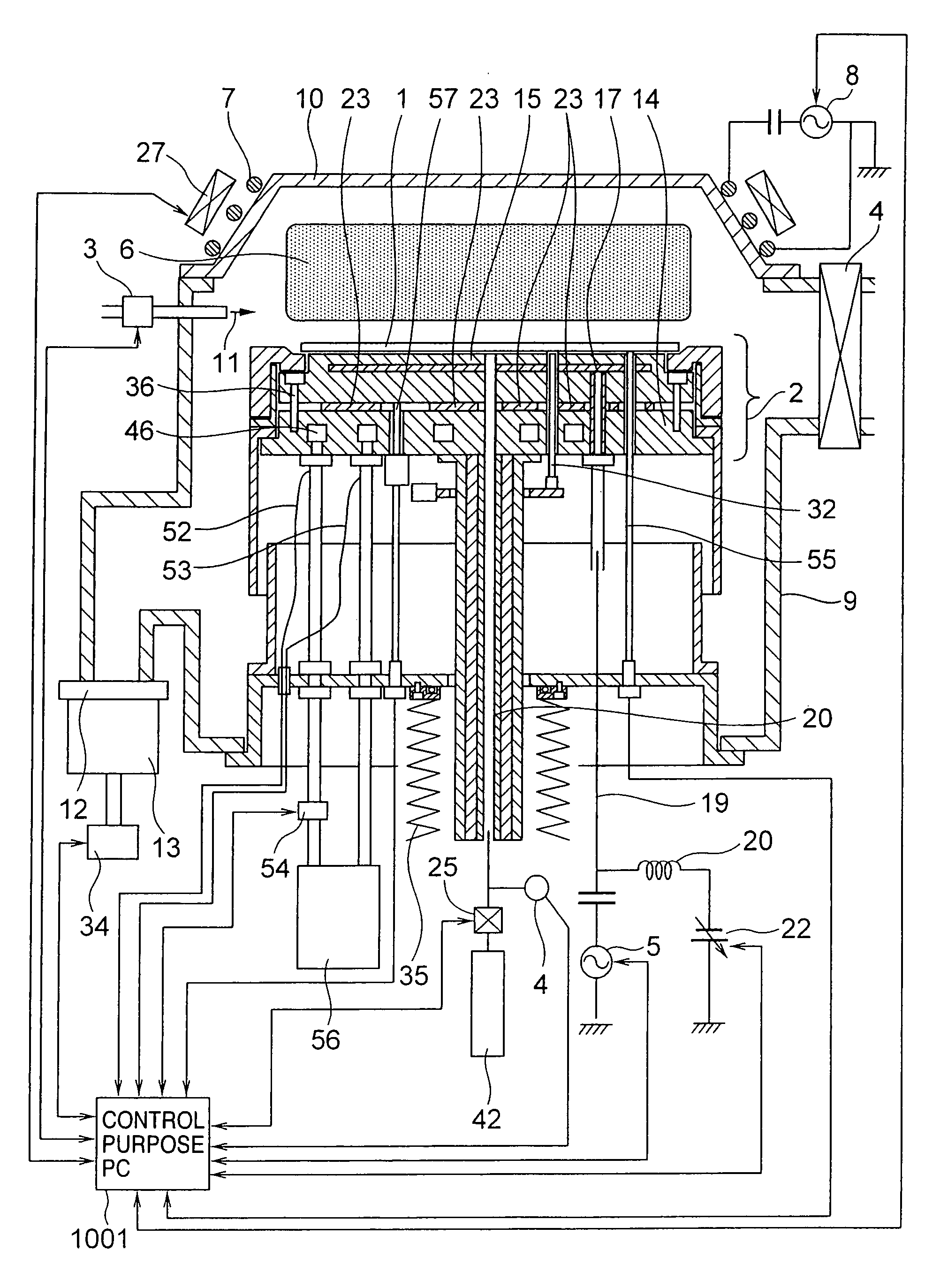
[0031] An embodiment of a wafer processing apparatus according to the invention will be described in detail with reference to the drawings. FIG. 1 shows one example of the etching apparatus to which this embodiment of the invention is applied.

[0032] Referring to FIG. 1, a wafer 1 is placed on a wafer stage 2 within a vacuum chamber 9. At this time, a bell jar 10 made of aluminum is secured to the top of the vacuum chamber 9 to keep the inside airtight.

[0033] The inside of the vacuum chamber 9 is evacuated by a turbo-molecular pump 13 and an oil-less pump 34, and then an etching gas 11 is introduced while it is being controlled in its flow rate by the flow controller 3. At this time, the inside of the vacuum chamber 9 is kept at a proper pressure by adjusting the opening valve travel of a valve 12 provided on the upstream of the turbo-molecular pump 13.

[0034] A coil 7 is provided to surround the bell jar 10, and a high-frequency voltage of, for example, 13.56 MHz is supplied to th...


PUM

PropertyMeasurementUnit
frequencyaaaaaaaaaa
flow rateaaaaaaaaaa
temperatureaaaaaaaaaa

Abstract

In a wafer processing apparatus, wafers are sequentially placed one by one on a ceramic plate of a wafer stage within a vacuum chamber. The pressure of a heat-conductive gas introduced at this time between the wafer and the ceramic plate is adjusted to control the temperature of the wafer, and the wafer is processed by use of plasma. In this case, the user can select any one of a process for regulating the pressure of the heat-conductive gas each time the wafers are sequentially placed on the wafer stage, a process for optimizing aging conditions, and a process for optimizing heater conditions so that the wafer temperature variation within lot can be reduced by performing the selected process. The selected process is performed on the basis of its conditions that are computed to determine by a control-purpose computer of the processing apparatus.

Description

CROSS-REFERENCE TO RELATED APPLICATION [0001] This application is a Divisional application of application Ser. No. 10 / 927,095, filed Aug. 27, 2004, the contents of which are incorporated herein by reference in their entirety.BACKGROUND OF THE INVENTION [0002] The present invention generally relates to techniques for etching semiconductor wafers, and particularly to a wafer processing apparatus of the system for continuously processing semiconductor wafers. [0003] Recently, as the semiconductor integrated circuit density increases, the circuit patterns formed in the semiconductor wafer have so far been entirely gone forward miniaturization and up to the point where the dimensional precision is required to be much stricter than ever. In this situation, the temperature management for the wafers (semiconductor wafers) during the process becomes extremely important. [0004] For example, in the etching process required for the patterns to have a high aspect ratio, an organic polymer is act...

Claims


Application Information

Patent Timeline
Patent Type & Authority Applications(United States)
IPC IPC(8): H01L21/306
CPCH01J37/32935H01L21/67248H01L21/67109H01J2237/2001
Inventor KANNO, SEIICHIROEDAMURA, MANABUUDO, RYUJIROARAI, MASATSUGUTANAKA, JUNICHIKANAI, SABURONISHIO, RYOJITSUBONE, TSUNEHIKOARAMAKI, TORU
Owner KANNO SEIICHIRO
Why Eureka
Try Eureka