Semiconductor storage device

a storage device and semiconductor technology, applied in semiconductor devices, semiconductor/solid-state device details, electrical apparatus, etc., can solve the problems of difficult to increase the capacity of the capacitor, the storage capacitor cannot be packed at maximum density, so as to achieve a high-density layout. , the effect of easy operation

Active Publication Date: 2007-10-18
LONGITUDE LICENSING LTD
View PDF3 Cites 42 Cited by
  • Summary
  • Abstract
  • Description
  • Claims
  • Application Information

AI Technical Summary

Benefits of technology

[0007]It is therefore an object of the present invention to provide a semiconductor storage device in which the storage capacitors can be arranged with maximum density in a 6F2 layout, and the HSG blockage margin can be adequately ensured.
[0009]According to the present invention, it is possible to arrange the storage capacitors at high density and adequately ensure the HSG blockage margin in a DRAM or other semiconductor storage device that has a 6F2 cell layout.
[0011]In the present invention, the center positions of the storage node contacts are preferably offset toward the corresponding bit line contacts in relation to the center positions of the second cell contacts, and are preferably offset so as to be at equal intervals in the X direction in relation to the center positions of the second cell contacts. All of the storage node contact pads can thereby be offset by the same amount, and it is easy to ultimately create a high-precision, high-density layout of the storage capacitors when the storage node contact pads are laid out at maximum density.
[0012]In the present invention, a first pad layout in which the positions of the storage node contact pads are offset in the direction towards the center portions of the corresponding active regions, and a second pad layout in which the positions of the storage node contact pads are offset in the direction away from the center portions of the corresponding active regions are preferably employed in alternating fashion for the plurality of active regions arranged in the Y direction. The first and second pad layouts are also preferably employed in alternating fashion for the plurality of active regions arranged on the straight line. In this case, the amount of offset of the storage node contact pads is preferably ¾F in the X direction and ⅓F in the Y direction. Offsetting the storage node contact pads in the manner described above makes it possible to arrange the storage node contact pads in a uniform zigzag pattern, and to easily achieve a high-precision, high-density layout of the storage capacitors.

Problems solved by technology

Therefore, the storage capacitors cannot be packed at maximum density.
However, in such a case as when the contact plugs are originally arranged in zigzag fashion in the transverse and longitudinal directions, it is difficult to pack the storage capacitors at maximum density.
Since the elliptical storage capacitors have an inadequate diameter in the minor axis direction, it is impossible to increase the capacity of the capacitors.
Furthermore, when the lower electrode of an MIS (Metal Insulator Silicon) capacitor is composed of HSG-Si (Hemi-Sphericai Grained poly-Si), the HSG blockage margin cannot be adequately ensured, and the cylinder holes used by the storage capacitors become blocked with HSG-Si.

Method used


Image

  • Semiconductor storage device
  • Semiconductor storage device
  • Semiconductor storage device

Examples


Embodiment Construction

[0042]Preferred embodiments of the present invention will now be described in detail hereinafter with reference to the accompanying drawings.

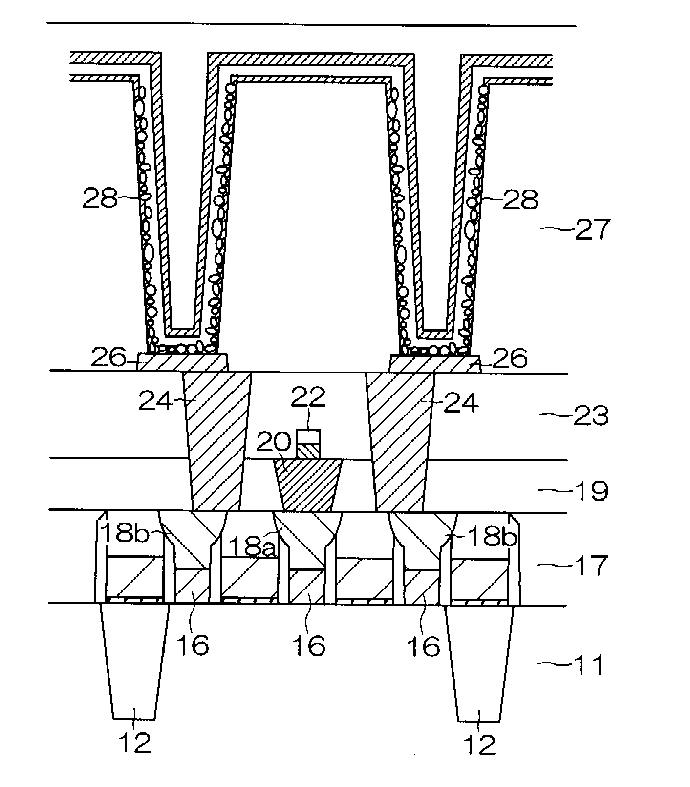
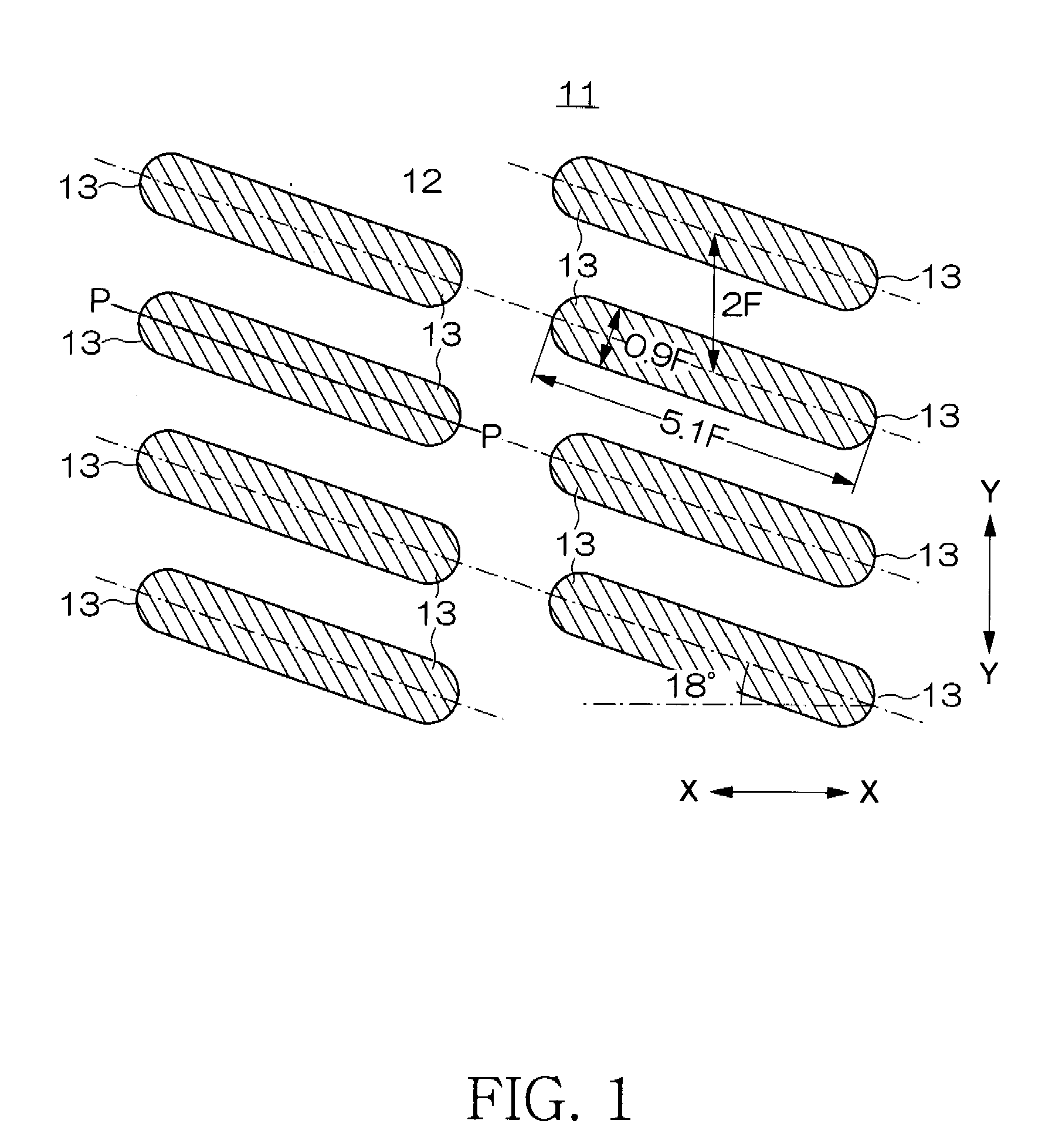
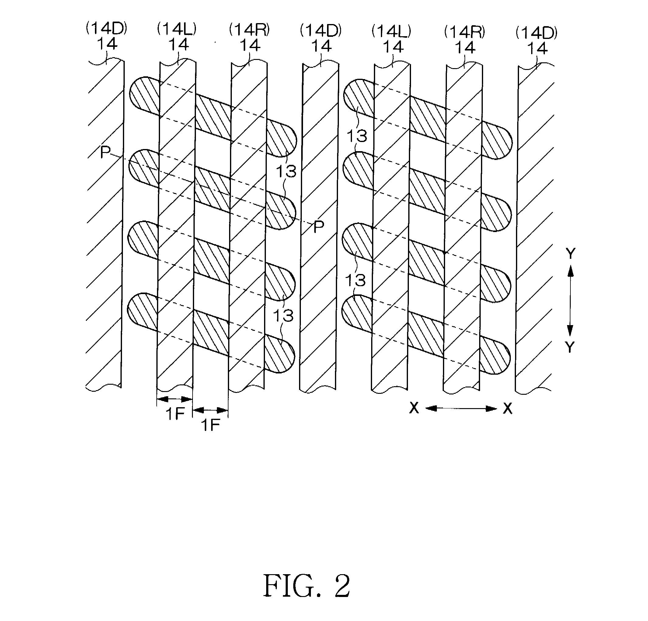
[0043]FIGS. 1 through 9 are schematic plan views showing the layout in the sequence of the manufacturing process of the DRAM 10 as an embodiment of the semiconductor storage device of the present invention. FIGS. 10 through 18 are schematic sectional views along line P-P in FIGS. 1 through 9, respectively.

[0044]In the manufacture of the semiconductor storage device 10, a field oxide film (element separation region) 12 is first formed by STI (Shallow Trench Isolation) or another method on a silicon substrate 11 as shown in FIGS. 1 and 10, whereby a plurality of active regions 13 is formed. The active regions 13 are substantially band-shaped regions having a prescribed length, and the plurality of active regions 13 is formed in a straight line in the longitudinal direction thereof. The longitudinal direction of the active regions 13 is angled app...


PUM


Abstract

a semiconductor storage device is provided with a plurality of active regions formed in the shape of a band in a semiconductor substrate; a plurality of word lines arranged at equal intervals so as to intersect the active regions; a plurality of cell contacts that includes first cell contacts formed in the active regions in the center portions in the longitudinal direction thereof, and second cell contacts formed at each end portion at both ends in the longitudinal direction; bit line contacts formed on the first cell contacts; bit lines wired so as to pass over the bit line contacts; storage node contacts formed on the second cell contacts; storage node contact pads formed on the storage node contacts; and storage capacitors formed on the storage node contact pads. The center positions of the storage node contacts are offset in a prescribed direction from the center positions of the second cell contacts. The center positions of the storage node contact pads are offset in a prescribed direction from the center positions of the storage node contacts.

Description

TECHNICAL FIELD[0001]The present invention relates to a semiconductor storage device, and particularly relates to a DRAM (Dynamic Random Access Memory) memory cell layout.BACKGROUND OF THE INVENTION[0002]In DRAM, which is one type of semiconductor storage device, a memory cell composed of a single transistor and a single capacitor is disposed at the intersection of a word line and a bit line that intersect with each other. Layout systems in DRAM memory cells are classified as folded bit line systems and open bit line systems (see Japanese Laid-open Patent Application No. 2004-80009). In a folded bit line system, two bit lines that are connected to a single sense amplifier are folded at the sense amplifier so as to be wired in the same direction, and the minimum theoretical area of the memory cell is 8F2 (4F×2F), wherein “F” is the minimum feature size (half the pitch of the word lines). In an open bit line system, two bit lines that are connected to a single sense amplifier are wire...

Claims


Application Information

Patent Timeline
Patent Type & Authority Applications(United States)
IPC IPC(8): H01L29/94H01L27/108H01L29/76H01L31/119
CPCH01L27/0207H01L27/10814H01L27/10855H01L2924/0002H01L2924/00H10B12/315H10B12/0335H01L29/40
Inventor HASUNUMA, EIJI
Owner LONGITUDE LICENSING LTD
Why Eureka
Try Eureka